

In my previous column, we discussed how the year 2030 seems set to be an exciting time to be in artificial intelligence (AI) and machine learning (ML) space (where no one can hear you scream). For example, in addition to the industrial IoT (IIoT) we also have the artificial intelligence of things (AIoT).
“What’s the AIoT when it’s at home?” I hear you cry. Well, according to the IoT Agenda, “The AIoT is the combination of AI technologies with the IoT infrastructure to achieve more efficient IoT operations, improve human-machine interactions, and enhance data management and analytics […] the AIoT is transformational and mutually beneficial for both types of technology as AI adds value to IoT through machine learning capabilities and IoT adds value to AI through connectivity, signaling, and data exchange.”
I’ve said it before and I’ll say it again, I couldn’t have said this any better myself.
As we noted in Part 1 of this 2-part miniseries, the folks at PwC project that the impact of AI on global GDP by 2030 will be around $15T. According to Forbes, the AIoT piece of this pie could be $1.2T in 2030. Meanwhile, the 2023 Edge AI Hardware Report from VDC Research estimates that the market for Edge AI hardware processors will be $35B by 2030.
All of this goes to explain why the folks at BrainChip are so excited by the recent announcement of their Akida 2.0 platform. As I mentioned in my earlier musings, the Akida is a fully digital neuromorphic event-based processor.
The first big point to note about this new incarnation is that it can run humongous models like ResNet-50 completely on the neural processor, thereby freeing up the host processor.
The second point you need to know is that, once you’ve trained your original model in the cloud, this platform supports the unique ability to learn on-device without cloud retraining, thereby allowing developers to extend previously trained models.
The third point that will excite those in the know is that the guys and gals at BrainChip have added spatial temporal convolutions and the innovative handling of time series data. This means that, in addition to traditional 2D data (like images), these features allow the Akida platform to treat various types of 1D and 3D data smartly, thereby enabling much better predictive analysis, video analytics, speech analysis, etc. All of this goes to provide better accuracy at the edge while substantially reducing models in terms of size and weights.
And the fourth big point is that the little scamps at BrainChip have added hardware support for vision transformers in the edge, thereby delivering a dramatic boost in machine vision performance.
What are vision transformers? I’m so glad you asked. Until recently, typical image processing systems like ResNet have employed convolutional neural networks (CNNs). In 2017, a transformer architecture was introduced for use in natural language processing (NLP), which involves analyzing, extracting, and comprehending information from human language. NLP includes both reading text and listening to spoken words.
In artificial neural networks (ANNs), the term “attention” refers to a technique that is meant to mimic cognitive attention (i.e., the concentration of awareness on some phenomenon to the exclusion of other stimuli). Transformers measure the relationships between pairs of input tokens (words in the case of text strings), and this is what we mean by attention in this context.
This concept was extended in 2019 into a vision transformer architecture for processing images without need of convolutions. The idea is basically to break down input images into a series of patches, which—once transformed into vectors—are essentially equivalent to the words processed by a normal transformer. The bottom line is that vision transformers can do a much better job of vision analysis by treating a picture like a sentence or a paragraph, as it were.
By “better” in this context I mean smaller and faster. How much smaller? How much faster? We will come to that in a moment. Before we go there, however, let’s first note that this latest incarnation of the Akida comes in three temptingly tasty flavors as shown below.
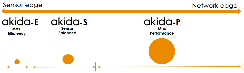
Akida: One platform for many scalable products (Source: BrainChip)
All of these flavors are intended for processing at the edge, but this leads us to the question, “What exactly is the edge?” In its broadest sense, the edge is where the internet meets the real world (where the rubber meets the road). For myself, I tend to think about the “extreme edge” or the “sensor edge” as being so close to the real world that you can smell it (assuming your sensor is of an olfactory nature, of course). By comparison, the “network edge” includes things like fog and mist computing in which edge devices (like servers) are used to carry out a substantial amount of computation, storage, and communication locally before ultimately connecting into the cloud.
The Akita-E, which has 1 to 4 nodes and provides up to 200 GOPS (giga operations per second), is targeted at low end sensor nodes. This can be run standalone or in conjunction with a min-spec MCU, and it’s ideal for always-on applications.
Next, we have the sensor-balanced Akita-S, which boasts 2 to 8 nodes and can provide up to 1 TOPS (tera operations per second). And for those applications demanding the maximum performance, we have the Akita-P, which flaunts (yes, I said “flaunts” and I’m not ashamed of myself) 8 to 128 nodes to deliver a squealing 50 TOPS (where the “squealing” qualifier would be me squealing in excitement). This bodacious beauty boasts temporal event-based neural nets and vision transformers. It has detection, classification, segmentation, and prediction. Basically, it can handle all types of complex networks with minimum CPU intervention.
Another way to look at this is as shown below. There are a bunch of simple AI/ML tasks like vibration detection, anomaly detection, keyword spotting, and sensor fusion that can be implemented using an MCU (although an MCU is not optimal, these tasks are certainly within its performance envelope). However, these tasks, which are shown in gray in the image below, could be better served using an Akida-E, which will be orders of magnitude more efficient.
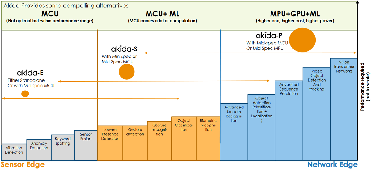
Example spectrum of edge AI/ML tasks and computational offerings (Source: BrainChip)
The applications shown as orange in the diagram cannot be implemented using MCUs by themselves; instead, they require some level of ML acceleration. These tasks can be easily accomplished using an Akida-S accompanied by a min-spec or mid-spec MCU.
Finally, we get to applications like speech recognition, gesture recognition, and object detection and classification, which are colored blue in the above diagram. Tasks of this ilk are usually performed using something like a Jetson (MPU+GPU) or a Snapdragon (AP+GPU). This is the application area where the Akida-P strides to the fore.
We don’t have the time (and I don’t have the energy) to take too deep a dive into the technology (rest assured that the folks at BrainChip will be delighted to talk your ears off if you ask them), but a super high-level view is as shown below.
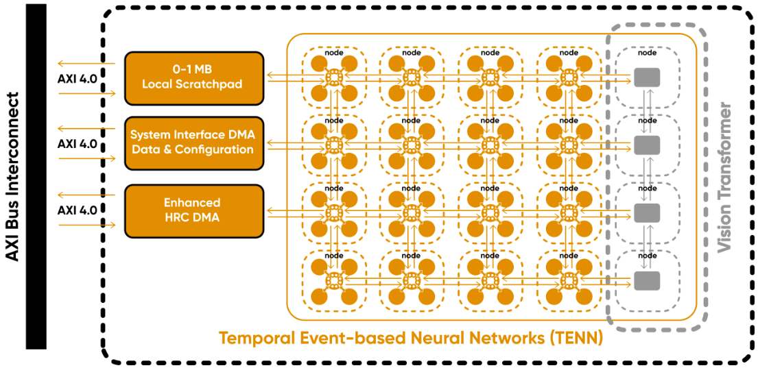
High-level architectural view of the Akida (Source: BrainChip)
Everything inside the dotted line is the IP that developers will integrate into their system-on-chip (SoC) devices. Communication with the rest of the SoC is realized via standard AXI bus interconnect. In addition to the temporal event-based neural nets (TENNs) and vision transformers, we have a local scratch pad memory, a system interface DMA, and an enhanced high resolution coding (HRC) DMA. This fully digital event-based design, which is portable across different foundries, accelerates all types of networks, including CNNs, DNNs, vision transformers, native SNN, and sequence prediction.
The Akida efficiently computes event domain convolutions, temporal convolutions, and vision transformer encoding. The DMAs supporting all of this minimize the load on the system and the host CPU because they access data when they need it, as opposed to relying on the CPU to manage everything when it has better things to do. Moreover, there’s an intelligent runtime software layer that handles everything transparent to the user.
One distinguishing characteristic of the Akida is its ability to support multi-pass processing, which means developers can implement more complex networks on smaller die areas. For example, suppose you have a complex and parallel network that would ideally be served by four Akida nodes. Now suppose you don’t have space budgeted on the die for this, in which case you could use a single node and perform multiple passes.
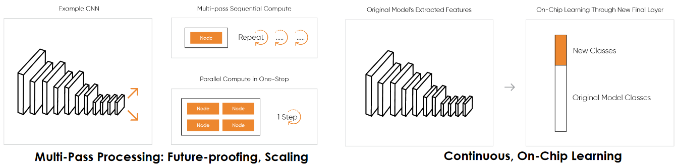 Additional features supported by the Akida (Source: BrainChip)
The great thing here is that the runtime software takes care of everything, such as performing segmentation, partitioning, and then running the multiple levels. Obviously, there’s latency involved, but this latency is minimized by having the runtime and the DMA take care of everything, which means the Akida doesn’t need to keep on transferring control back to the CPU.
As we previously noted, the Akida also supports continuous on-chip learning, which allows developers to use existing trained models, extract features, and then extend classes on the last fully connected layer. All of this customization is performed on the device without the need for cloud retraining.
In the case of vision transformers, the Akida supports the encoder block fully in hardware. This encoder block is fully contained and—once again—managed by DMA and runtime software. Just to give a sense of what this means, two nodes running at 800MHz provide 30 frames per second performance for high resolution video, which is compelling for an edge device.
Another new feature is the concept of temporal event-based neural nets, which are easy to train and extremely data efficient. The idea here is to regard 3D data as spatial frames with a temporal component, and to train the network with back propagation like a CNN, extracting both spatial and temporal kernels. Subsequently, when inferencing, the system employs the spatial kernel as a 2D frame and the timing aspect, which is the third dimension, as a recurrent inference. The result is to facilitate tasks like object and target tracking.
Yet another way all of this becomes interesting is when dealing with 1D data or signals. For example, the Akida is extremely effective when working on things like raw audio signals or health care signals.
And so we come to the old proverb that states, “The proof of the pudding is in the eating.” Just how well does the Akida perform with industry-standard, real-world benchmarks?
Well, the lads and lasses at Prophesee.ai are working on some of the world’s most advanced neuromorphic vision systems. From their website we read: “Inspired by human vision, Prophesee’s technology uses a patented sensor design and AI algorithms that mimic the eye and brain to reveal what was invisible until now using standard frame-based technology.”
According to the paper Learning to Detect Objects with a 1 Megapixel Event Camera, Gray.Retinanet is the latest state-of-the-art in event-camera based object detection. When working with the Prophesee Event Camera Road Scene Object Detection Dataset at a resolution of 1280×720, the Akida achieved 30% better precision while using 50X fewer parameters (0.576M compared to 32.8M with Gray.Retinanet) and 30X fewer operations (94B MACs/sec versus 2432B MACs/sec with Gray.Retinanet). The result was improved performance (including better learning and object detection) with a substantially smaller model (requiring less memory and less load on the system) and much greater efficiency (a lot less time and energy to compute).
As another example, if we move to a frame-based camera with a resolution of 1352×512 using the KITTI 2D Dataset, then ResNet-50 is kind of a standard benchmark today. In this case, Akida returns equivalent precision using 50X fewer parameters (0.57M vs. 26M) and 5X fewer operations (18B MACs/sec vs. 82B MACs/sec) while providing much greater efficiency (75mW at 30 frames per second in a 16nm device). This is the sort of efficiency and performance that could be supported by untethered or battery-operated cameras.
Another very interesting application area involves networks that are targeted at 1D data. One example would be processing raw audio data without the need for all the traditional signal conditioning and hardware filtering.
Consider today’s generic solution as depicted on the left-hand side of the image below. This solution is based on the combination of Mel-frequency cepstral coefficients (MFCCs) and a depth-wise separable CNN (DSCNN). In addition to hardware filtering, transforms, and encoding, this memory-intensive solution involves a heavy software load.
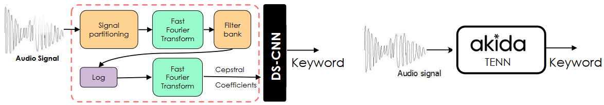
Raw audio processing: Traditional solution (left) vs. Akida solution (right)
(Source: BrainChip)
By comparison, as we see on the right-hand side of the image, the raw audio signal can be fed directly into an Akida TENN with no additional filtering or DSP hardware. The result is to increase the accuracy from 92% to 97%, lower the memory (26kB vs. 93kB), and use 16X fewer operations (19M MACs/sec vs. 320M MACs/sec). All of this basically returns single inference while consuming two microjoules of energy. Looking at this another way, assuming 15 inferences per second, we’re talking less than 100µW for always-on keyword detection.
Similar 1D data is found in the medical arena for tasks like vital signs prediction based on a patient’s heart rate or respiratory rate. Preprocessing techniques don’t work well with this kind of data, which means we must work with raw signals. Akida’s TENNs do really well with raw data of this type.
In this case, comparisons are made between Akida and the state-of-the-art S4 (SOTA) algorithm (where S4 stands for structured state space sequence model) with respect to vital signs prediction based on heart rate or respiratory rate using the Beth Israel Deaconess Medical Center Dataset. In the case of respiration, Akida achieves ~SOTA accuracy with 2.5X fewer parameters (128k vs. 300k) and 80X fewer operations (0.142B MACs/sec vs. 11.2B MACs/sec). Meanwhile, in the case of heart rate, Akida achieves ~SOTA accuracy with 5X fewer parameters (63k vs. 600k) and 500X fewer operations (0.02B MACs/sec vs. 11.2B MACs/sec).
It’s impossible to list all the applications for which Akida could be used. In the case of industrial, obvious apps are robotics, predictive maintenance, and manufacturing management. When it comes to automotive, there’s real-time sensing and the in-cabin experience. In the case of health and wellness, we have vital signs monitoring and prediction; also, sensory augmentation. There are also smart home and smart city applications like security, surveillance, personalization, and proactive maintenance. And all of these are just scratching the surface of what is possible.
Another thing I’ve said before, and I will doubtless say again, is that we certainly do live in interesting times. How about you? What do you think about all of this?


Sounds like a new dominant player in the edge AI space. Nobody even close to what Brainchip is doing!
There are now so many things going on in AI space (where no one can hear you scream) that I’m finding it difficult to wrap my poor old brain around everything)
Official ML Commons Tiny benchmark results: https://mlcommons.org/en/inference-tiny-10/
Brainchip white paper with selected non verified results: https://brainchip.com/wp-content/uploads/2023/01/BrainChip_Benchmarking-Edge-AI-Inference-1.pdf
Dominant player?
I noticed the benchmarks appear to be against MCUs. There are other edge-targeted inference devices being offered as well, including recent low-power FPGAs. Bottom line, many competitive strategies in a dynamic, green fields market.