


Processors and FPGAs go together like chocolate and peanut butter, but it took a few years to get the recipe just right. Early turn-of-the-millennium attempts included the Xilinx Virtex II Pro with an on-chip PowerPC processor core and Altera’s Excalibur device with an ARM922T processor core. These early products are considered market failures. Actually, Kevin Morris called the Altera Excalibur “a monumental flop” in his article titled “Shaking Up Embedded Processing.” Why? Because you can’t just plop an unconnected microprocessor core into the middle of an FPGA array and call it a finished product. There’s simply no added value there. Few designers want to waste time designing some sort of bog standard processing subsystem around a naked processor core, and no one wants to use precious, programmable LUTs to implement that processor subsystem once it’s designed.
The current trend of merging processor cores with hardened microprocessor subsystems together with FPGAs on one chip started early in 2010. Xilinx first revealed the Zynq “EPP” (Extensible Processing Platform) architecture during a short presentation at the Real Time & Embedded Computing Conference (RTECC) held in Santa Clara, California on January 26, 2010. (See Dick Selwood’s article titled “A Platform to Bridge a Gap?”)
EPP? Ecch.
The original Xilinx Zynq-7000 EPP family was based on a dual-core Arm Cortex-A9 application processor. Since then, single-core Zync SoCs have been added to the original family, and the family has matured with the introduction of Zynq UltraScale+ MPSOCs, which provide a mix of Arm Cortex-A53 application processor cores and Arm Cortex-R5 real-time processor cores. Thankfully, Xilinx’s EPP moniker didn’t stick around very long. As Dick Selwood wrote, “Extensible Processing Platform doesn’t really have a zing to it, does it?” But the concept itself had real staying power.
Xilinx’s arch rival, Altera, quickly introduced a very similar product and dubbed it the “SoC FPGA.” I’m not convinced that “SoC FPGA” has any more zing to it than “EPP,” but Altera’s name for this new device class stuck. It has become synonymous with devices that merge processors and FPGAs on one piece of silicon. Although Altera’s “SoC FPGA” continues, Altera has now been acquired by Intel, and the Altera brand itself is just finishing its slow fade into oblivion.
The first Xilinx Zynq EPP device finally shipped at the very end of 2011, and Altera shipped its first SoC FPGAs about a year later. Today, both companies have diverse product lines that combine Arm processor cores (anywhere between one and six of them, so far) with other hardened microprocessor peripherals, on-chip memory, and varying amounts of FPGA fabric.
SoC FPGAs solve some real engineering challenges, which explains their growing popularity. Microprocessors executing software are simply too slow to implement many high-speed tasks. That’s where you need an FPGA. There are distinct advantages to putting the processor cores and FPGA fabric down on one piece of silicon. The chief advantage is the immense jump in bandwidth you get between the processor and the FPGA.
The original Zynq-7000 series had more than 3000 on-chip connections between the FPGA fabric and the processor subsystem. That’s far more connectivity than you can achieve when wiring between packages over a pcb. In addition, those on-die connections in an SoC FPGA consume far less power because the drivers for those signal lines need not drive pcb traces. So, SOC FPGAs offer more connections, faster connections, and less I/O power – pick any three.
Microsemi entered the fray early too
Microsemi has also offered products in the SoC FPGA category for quite a while with its SmartFusion and SmartFusion 2 SoC FPGAs. Both are based on the Arm Cortex-M3 processor core. Microsemi introduced the SmartFusion 2 SoC FPGA in late 2012, but the original SmartFusion device was announced by Actel in March of 2010, just a couple of months after Xilinx announced the Zynq EPP and about half a year before Microsemi acquired Actel. (See Jim Turley’s “Actel’s Three-Legged Stool.”) Microchip subsequently acquired Microsemi in May, 2018. Big fish continue to eat the smaller fish in the semiconductor world.
SmartFusion devices are unique in the SoC FPGA category for at least two significant reasons. First, they incorporate Flash memory, both for the on-chip processor’s instruction and data memory and for the FPGA’s configuration memory. Use of on-chip, Flash-based configuration memory means that SmartFusion SoC FPGAs power up “instantly” as configured devices. These devices do not download their FPGA configuration from an attached serial EEPROM. They’re configured as soon as power is available.
Microsemi’s SmartFusion devices are also unique among SoC FPGAs because of their Arm Cortex-M3 processor cores, which are designed to be used as simpler 32-bit microcontroller cores. Although the Arm Cortex-M3 processor core has a memory-protection unit, it lacks an MMU. That means it’s not able to run a big operating system like Linux, although it certainly can run an RTOS.
In addition, the Arm Cortex-M3 has a 3-stage pipeline, which means it doesn’t run very fast. The SmartFusion and SmartFusion 2 devices run their Arm Cortex-M3 processors at 166MHz. That’s fast for a microcontroller, but mighty slow for an application processor. The multiple Arm Cortex-A series application processor cores incorporated into SoC FPGAs from Intel and Xilinx have full-blown MMUs and operate on clocks that are 5x to nearly 10x faster than the SmartFusion devices’ 166MHz Arm Cortex-M3 processor.
So the original SmartFusion and SmartFusion 2 devices weren’t designed to compete in the same weight class as the Intel and Xilinx parts. Both of these differentiators indicate that SmartFusion devices target embedded applications where microcontrollers might otherwise be used. However, the on-chip FPGA allows SmartFusion devices to outperform any conventional microcontroller.
The RISC-V Love Fest
Earlier this month, at the first RISC-V Summit (aka “open-source processor love fest”), Microsemi announced a significant upgrade to the SmartFusion device concept by announcing its PolarFire SoC FPGA architecture. (No actual parts yet announced.) The block diagram for this architecture appears in Figure 1 below.
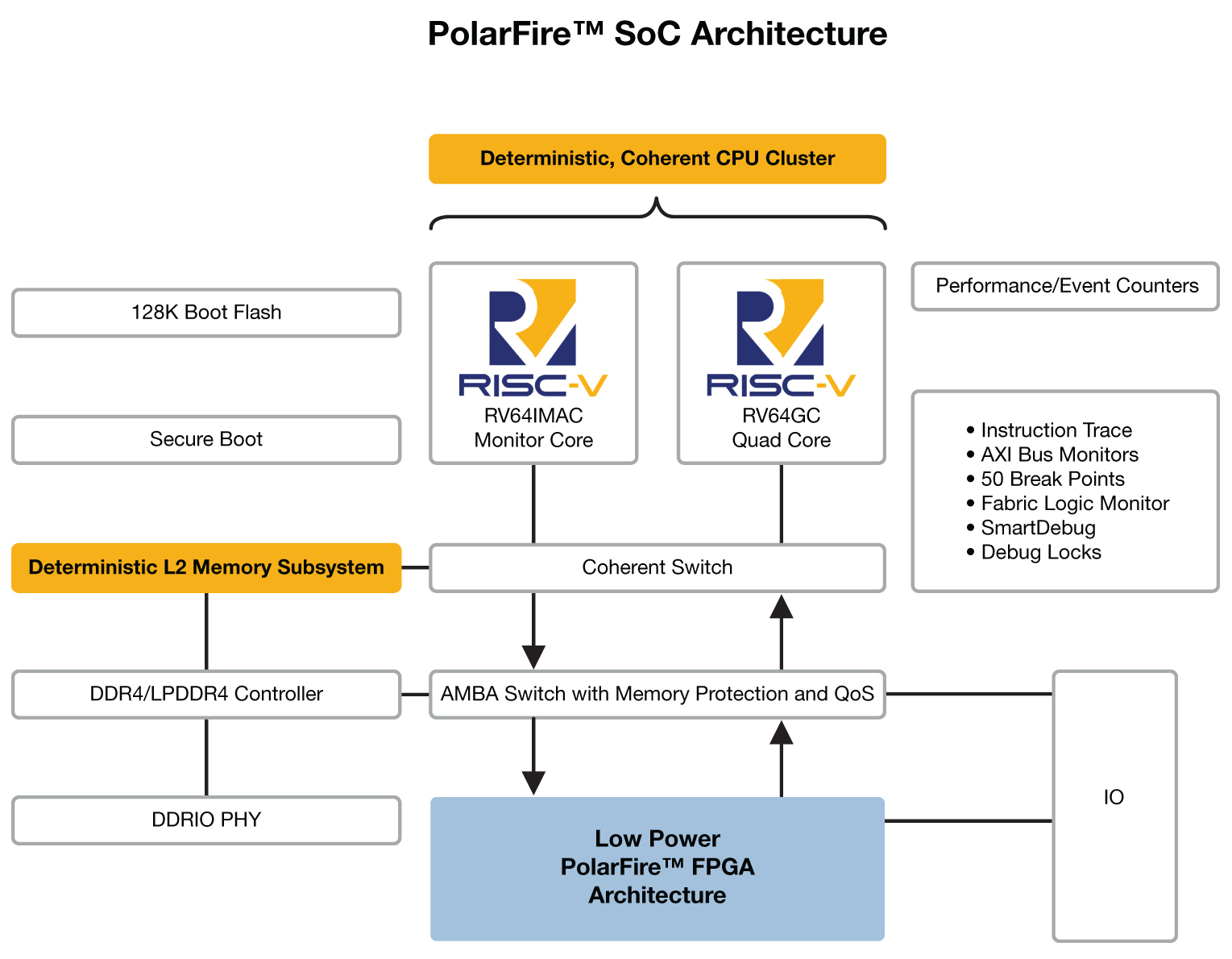
Figure 1: Microsemi’s PolarFire SoC architecture mates five 64-bit, RISC-V processor cores with assorted peripherals, on-chip Flash memory, a 2Mbyte “deterministic” L2 cache memory, a DDR4 SDRAM memory controller, and a block of the company’s PolarFire FPGA.
At first blush, the PolarFire SoC architecture shown in Figure 1 appears to have two RISC-V processor cores. However, the two blocks marked “RISC-V” in the Figure are significantly different. The block on the left represents a single RISC-V processor core that implements a 64-bit RISC-V RV64IMAC architecture with the standard integer, integer multiplication and division, atomic, and compressed instruction sets. Although it’s called a “monitor core” in the diagram, it’s a 64-bit integer processor that’s quite capable of executing real-time tasks. This processor core is a SiFive E51 core.
The processor block on the right in Figure 1 represents a quad-core RISC-V RV64GC processor with the standard RISC-V “general” instruction set including integer, integer multiplication and division, atomic, single- and double-precision floating-point, and compressed instructions. So this right-hand block represents four 64-bit processor cores, each with built-in floating-point hardware. This processor core is a SiFive U54-MC core.
The PolarFire SoC’s five 64-bit processor cores all communicate through a common, 2Mbyte L2 cache with some unusual properties that earn it the name “Deterministic L2 Memory Subsystem.” The L2 memory is partitioned into eight chunks, and seven of the chunks can be designated as cache, as a coherent scratchpad buffer, or as direct-access memory as shown in Figure 2. This L2 flexibility enables many real-time configurations for the processors.
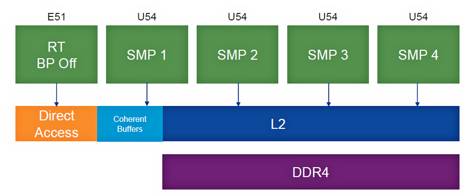
Figure 2: The PolarFire SoC’s five 64-bit RISC-V processor cores communicate to DDR4 SDRAM through a configurable L2 Memory Subsystem with deterministic properties.
The PolarFire SoC’s 4+1 processor subsystem closely resembles the design of SiFive’s Freedom U540 SoC (unfortunately designated FU540), which is available on SiFive’s HiFive Unleashed RISC-V dev board. This board can be plugged into a Microsemi-developed companion board called the HiFive Unleashed Expansion Board, which carries a Microsemi PolarFire FPGA. Together, the two-board set closely approximates the PolarFire SoC architecture, with about 98% of the capabilities of the yet-to-be-announced device, according to Microsemi.
The significant architectural feature remaining for discussion is the connection between the PolarFire SoC architecture’s processor complex and the on-chip FPGA. Figure 1 above represents that connection with two skinny, little unidirectional arrows. If those thin arrows were accurate, then communications between the five 64-bit RISC-V processor cores and the FPGA would be severely restricted, and that would negate the entire reason for putting the processors and FPGA on the same die.
So I asked.
Those two skinny, little arrows represent multiple 64-bit AXI buses, so there’s “plenty of bandwidth” between the processor complex and the FPGA, according to Microsemi. How much bandwidth? Microsemi won’t say at this time, because this is an architectural announcement, not a product announcement.
The Tool Factor
And finally, there’s the question of tools. SoC FPGAs are hybrid animals. They’re part processor and part FPGA. For the processors, you need the standard suite of development tools: compilers, assemblers, linkers, debuggers, instruction-set simulators, profilers, etc. The greater RISC-V community is quite busy developing these tools, and the support ecosystem for RISC-V software development is undergoing superluminal expansion at the moment. The number of registered members participating in the RISC-V Foundation doubled from 2017 to 2018. There are now more than 200 corporate and individual members contributing to the growth of RISC-V according to the Foundation’s Executive Director Rick O’Connor.
For FPGA development, Microsemi offers the same Libero PolarFire Design Suite that it offers for its PolarFire FPGAs. Libero integrates two strong FPGA development tools: Synopsys’s Synplify Pro ME synthesis tool and Mentor Graphics’ ModelSim ME simulation tool. These are fine FPGA development tools.
However, there’s something missing in the tool domain, so I asked about that. I wanted to know how system developers using the PolarFire SoC architecture can easily accelerate a software-based task by moving the task to an FPGA-based hardware accelerator. The answer: it must be coded as you’d code any hardware block by manually writing HDL code and then writing the corresponding software drivers. There’s no automation. I asked “Why?”
Now there’s a get-out-of-jail free answer to that question: “We’re working on it.”
That’s not the answer I got from Microsemi. The answer I got was “Our customers haven’t asked for that.”
OK, then.
There are lots of goodies to attract designers to Microsemi’s PolarFire SoC. First and foremost, there’s the allure of RISC-V, today’s poster child for the open-source hardware movement. There’s the Flash-based FPGA configuration, which is an attractive feature for many embedded designs because it confers instant-on capability. The Flash configuration memory is also touted as “SEU-immune,” so it’s great for high-reliability applications.
However, when it comes to tools, Microsemi has a lot of distance to make up. Compared to the Arm ecosystem, the RISC-V support ecosystem is immature. However, RISC-V Foundation Executive Director Rick O’Connor predicted a lot of ecosystem growth over the next year during an interview at the recent RISC-V Summit. Let’s hope so. In addition, the lack of bridge design tools that permit easy transition from software-based task execution on microprocessors to hardware-accelerated tasks in the PolarFire SoC’s FPGA puts Microsemi far behind Intel and Xilinx in the tool department.
Run Microsemi, run.


There would be somewhat more value in RISC-V if it was something more than just the latest rev of an old idea, but done cheaper.
In the pictures above it could be a number of CPUs in the “RISC-V” boxes, and it would work just the same – most of the buses seem to be ARM tech.
Does this mean the computer engineering community are just out of ideas?
Kev, It is the user community that has been so brain washed that new ideas are not welcome.
I think “RTL” means that the only choices for design entry are VHDL and Verilog. RISC V is ancient and just one more that loads each operand, fetches an instruction that does the operation, then stores the result.
Before RISC an instruction typically had an op code and an operand address so the address and data only needed one memory access. And they did multiply and divide without making a big deal out of it.
Here’s an idea: Build a computer that resembles a GPU that takes a chunk of data and processes it using if/else, for, while, do and pipe-lined assignment evaluation. That is WITHOUT COMPILING down to a mickey mouse ISA and beating memory to death fetching load and store instructions. By the way since the data can be streamed, there is no need for cache either. Actually the program can also be streamed out because of the memory that can be put on a chip.