


The upshot: Optima claims to have accelerated functional-safety fault coverage by 1000x, making possible large ASIL-D chips.
Functional safety is the new headache on the block. Once reserved for mil/aero designs only, automobiles have now shoved it into the spotlight. We’ve talked about it before, but much of the discussion, perhaps not always explicitly stated, had practical impact mostly for lower-ASIL designs – that is, for less safety-critical components. We’ve never addressed ASIL-D – the highest level, applying to things like engine control and braking – directly.
But a conversation with newly-launched Optima brought ASIL-D front and center. The kind of analysis required to document greater than 99% fault coverage – required for ASIL-D – simply takes too long for large chips, meaning that only small chips – mostly on 180-nm processes (and restricted to 90 nm for single-event upsets, or SEUs) – qualify for an ASIL-D rating.
They say that each gate must be simulated 6 times (stuck-at 1/0 on 2 inputs and an output). So, as an example, a small-medium chip of 100 million gates, simulating at 1 minute per run, takes 600 million minutes, or just over a thousand years, to analyze. That probably breaks the time-to-market window. As a result, either emulation is required (with multiple emulators running in parallel – expensive!) or the designs are sampled rather than being analyzed exhaustively. Using that approach, you can’t get to 99% fault coverage – by definition.
Optima’s fundamental claim to fame is their new FIE (fault-injection engine) toolset, which accelerates this process to just over a year for that example design – on a single core. You can then use parallelism to bring it well within range, and now you have a pathway to producing larger ASIL-D chips.
They’ve done this by redoing the algorithms from the ground up, leveraging a combination of simulation and formal analysis. They claim new fault-pruning and fault-collapsing techniques, which reduce the size of the problem before the hard computing starts. They can operate both at the RTL level, where you can do estimates, and at the netlist level for final checkout.
Classifying Circuits
Before we go into what the tools do, it’s instructive to look at the different categories of possible fault, since some of this isn’t obvious if you’re new to the safety game. The idea here is that, ultimately, you’re going to have your main circuit logic, and then you’re going to have safety mechanisms that detect faults as they occur. Optima has a drawing that they use, and they were kind enough to break it down to help illustrate the concepts.
The main logic has a cone of influence (CoI): this is all of the logic that contributes to an output. Think of it as a watershed, defined by all the streams and creeks that ultimately feed into a specific river. This CoI is shown next.
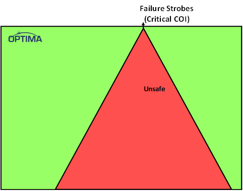
(Image courtesy Optima)
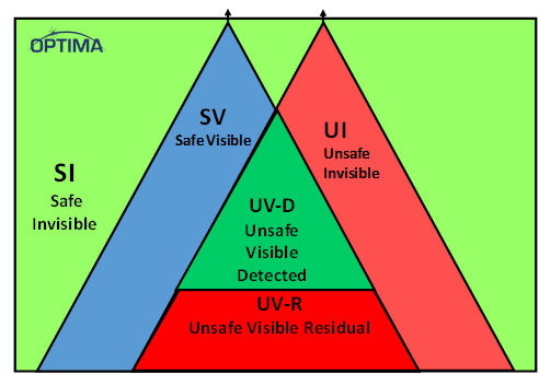
There are two things to note here. First, the outputs are cryptically referred to as “failure strobes.” I find that confusing, since, in the application, these aren’t strobes that activate when a failure has occurred. They’re the signals that could fail, and, if they did so, it would create a safety issue. Optima suggested thinking of them as “critical signals.” By definition, then, these signals are considered to be unsafe if they’re not protected by a safety mechanism. The green around the CoI represents other logic – logic that isn’t a safety issue, so it’s all safe – by definition.
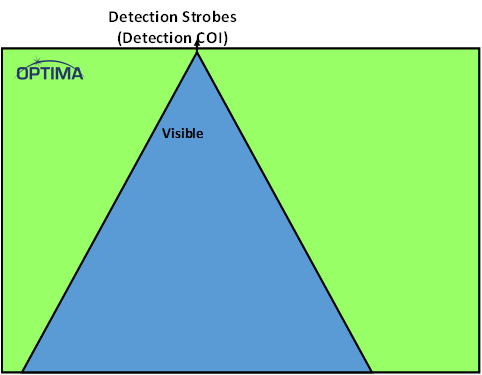
The above image assumes that there are no safety circuits; next we would put those in. They also have a CoI, shown next. Optima refers to the outputs of the safety circuits as detection strobes, since they will indicate whether or not a failure has been detected. That said, some safety circuits don’t have an output – in fact, some correct errors. In that case, a fault wouldn’t propagate to the outputs because it’s been corrected.
(Image courtesy Optima)
This drawing also illustrates another notion: that of visibility. In this context, a visible fault is one that can be detected by a safety mechanism. This shows that, by definition – almost – the safety circuits are visible. I say, “almost” because, in fact, safety circuits can also have faults, and you might want to detect them, so there might be a bit of onion-peeling here, with safety mechanisms to detect main logic issues, more mechanisms to detect safety mechanism issues, and more mechanisms for those… It’s asymptotic that way, but you never get to 100% coverage anyway, really, so you just need to get above the 99% level
So now we have these two CoIs in the same chip, and, in fact, they overlap. There’s no way they will ever coincide exactly, since the safety mechanisms will involve some circuits that aren’t part of the main CoI, and it may be that there are bits of the main Coi that aren’t covered. The non-overlapping parts of the safety CoI are considered safe, so they’re noted as safe visible. The non-overlapping parts of the main CoI, however, represent unsafe invisible logic, and you want to minimize that space.
The overlapping region is logic that is covered by safety mechanisms, so it’s unsafe visible, meaning that they’re critical circuits that can cause a problem if there’s a fault, but any faults will now be visible because it intersects with the safety CoI.
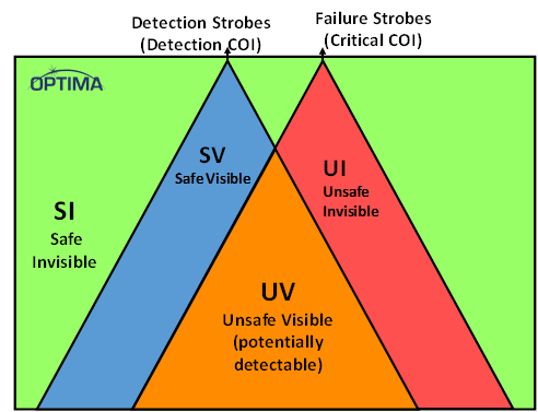
(Image courtesy Optima)
The remaining question is whether faults within this region are truly detected. That makes for two main steps for the analysis: first, static analysis and formal techniques are used to establish the CoIs and the overlap region. The second step is to prove that the safety circuits in the overlap region can detect >99% of the possible faults. That’s a job for fault injection and simulation.
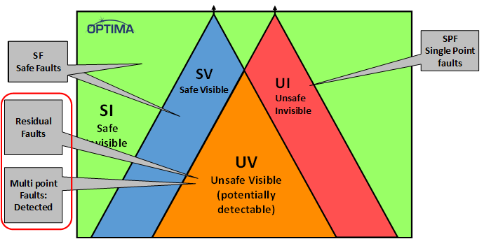
There are apparently some terms of art in the FMEDA (Failure Modes, Effects, and Diagnostic Analysis) world that relate to these regions, and Optima provided a “map” for that.
(Image courtesy Optima)
After fault analysis, you end up with a subregion of faults that were detected by the safety circuits and residual faults that haven’t been detected. The detected region has to be above 99%.
(Image courtesy Optima)
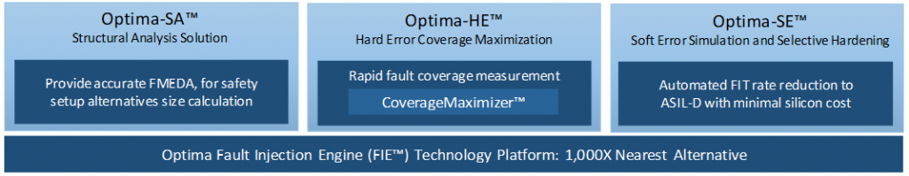
Three Tools in the Chest
Optima FIE consists of three tools: one for the initial analysis that identifies the CoIs, one for dealing with hard errors, and one for dealing with soft errors.
(Image courtesy Optima)
Let’s start by reviewing the hard- vs. soft-error thing. Hard errors refer to a permanent condition: signal stuck at 1 or 0. (Bridging is also a possible condition, but, according to Optima, no one can cover that yet; it’s on their roadmap.) One thing that’s easy to get confused about is how such errors could have escaped testing in the first place. Why weren’t chips with stuck-at faults rejected?
Because we’re not talking about manufacturing faults here; we’re talking about faults that arise after a good chip has been installed in a system. Perhaps there was a voltage glitch, or maybe there was an issue with some environmental factor. The assumption, then, is that the fault persists. And the analysis question is, “If such a fault were to arise, would it have a visible effect?” That’s what the fault-injection thing is all about: replacing a known good node with a faulty node and seeing if the fault is detected.
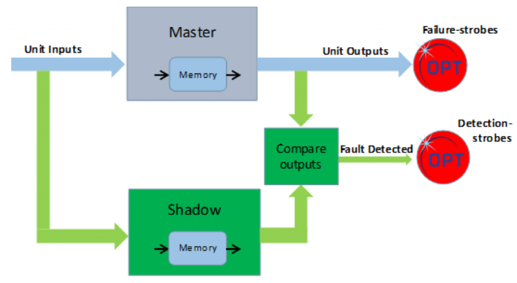
Then there are the soft (or transient) errors: these are signals in the system that get perturbed for some reason – alpha particles or other SEUs – and which can recover, even if simply through a power cycle. While a hard error may render a system permanently unusable (with the challenge being to take the system down safely), a soft error can possibly be accommodated – if it can be detected when it happens. Such detection (but not correction) can happen via so-called dual-core lockstep redundancy (also referred to as dual-mode redundancy, or DMR). If the master and shadow circuits below don’t agree, then it’s an indication that something is wrong.
(Image courtesy Optima)
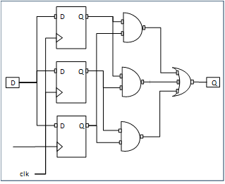
Soft errors can even be corrected using triple-module redundancy (TMR), although that uses much more silicon, making it more expensive.
(Image courtesy Optima)
The scope of what can be covered by DMR is a matter of some discussion. Classically, it’s used for a CPU and associated logic – in other words, a big chunk. That’s because it creates a detection output that has to be routed out somehow. TMR, on the other hand, can be used at the register level more easily because it has no output; it corrects the signal.
In a separate discussion with Arteris regarding their CodaCache IP, they mentioned that they use DMR at a level lower than the CPU level (since it’s not a CPU circuit). But they don’t go all the way down to the register level. The issue of routing the detection strobes is a matter of how communication happens on a chip. If you’re using a network-on-chip (NoC), the circuit might initiate a detection message on the network, meaning that there’s not an additional signal that has to be routed across the chip. Or, performance permitting, you could theoretically have a single detection strobe connected to all detectors in a wired-OR configuration. That still might create a burden (especially if you have to segment the line for performance), so the main point of this is that the scope of DMR has to be carefully considered by the designer.
The Optima FIE Flow
We take the three tools and run them in order, starting with Optima-SA, which creates a minimal fault list. This is a standard capability of similar tools already available, although there may be some differences based on how well Optima-SA does fault pruning and collapsing as compared to other tools. Optima’s version runs in less than an hour.
The main differences from existing tools come from the follow-on analysis done on that list for hard and soft errors. Optima-HE analyzes the chip to ensure that the safety mechanisms in place are providing enough coverage – a necessary step for proving to the ISO-26262 masters that coverage is sufficient to attain an ASIL-D rating. If coverage is too low, their CoverageMaximizer tool provides recommendations on how to improve it.
Optima-SE, meanwhile, analyzes all of the flip-flops to determine where “hardening” is required. Hardening can be as simple as making a flip-flop more resistant to metastability or as expensive as TMR. Any hardening has some cost, so you want to restrict hardening to the fewest possible flip-flops. Optima-SE helps with this by calculating an Architectural Vulnerability Factor, or AVF, to each flip-flop. This amounts to figuring out the failure-in-time (FiT) rate of that flip-flop on its own. From here, you can then calculate the overall FiT rate that would result if high-AVR flip-flops were hardened. Optima says that, prior to Optima-SE, these calculations would take many months.
The tool doesn’t automatically insert hardening circuitry; it’s still up to the designer to implement the changes. The benefit of the tool is to identify a minimal set of flip-flops – those having the most impact. That allows a more surgical repair. Note, however, that DMR is a less likely solution here, since this operates at the flip-flop level, and DMR isn’t usually used at that low a level.
Some of Optima’s materials show -SA running first, then -HE, and then -SE, in that specific order. While -SA does indeed have to run first, the other two can be run in either order. Apparently, there’s a historical tendency to do -HE first, but it’s by no means required.
After all of this discussion of safety notions, it’s perhaps useful to back out once more to remind ourselves of what’s new here. The theoretical benefit of doing all of this is well known. The problem has been the time it takes to run the analysis. So, the specifics of how each tool works aside, the fundamental change here is the dramatic improvement in analysis time, raising the complexity of chips that can be incorporated into a safety-critical design without compromising that safety.
More info:
Sourcing credit:
Jamil Mazzawi, Founder and CEO, Optima


What would you build if you could get a large automotive SoC to qualify for ASIL-D?
I will be very happy to answer any question about the article and the Optima Safety Platform.
Just post the question as a comment bellow