

Rarely does a day go by without my taking a few moments to reflect on how wonderful I am. I’m not talking about my outrageously good looks or my internationally commented-on sense of style (although I’m not discounting these, either), but rather the fact that I—and you, if we’re being honest—are biological marvels.
Take our long-range visual sensing capability and consider what happens when we are travelling at speed in a car bouncing along a bumpy road, for example. The combination of our biological optical sensors (eyes), inertial measurement sensors (inner ears), and processing unit (brain) is so powerful that we typically don’t even think about the bouncing motion of the car unless it’s excessive. We simply filter out any extraneous noise inputs and continuously perform object detection and recognition, along with other activities like predicting the future (deciding what’s likely to happen next based on what we’re seeing now).
The reason for my current cogitations and ruminations is that I was just chatting with Eric Aguilar, who is CEO and Co-Founder of Omnitron Sensors. Although this is a small company that’s only just come out of stealth mode, the folks at Omnitron may be poised to shake up the MEMS sensor market. This isn’t too surprising when we learn that their executive team has spent decades in sensor design, working on projects at Google (X) Wing avionics, Google Quantum, Tesla Model 3, US Navy Research Labs, and Lumedyne (which was acquired by Google). For example, Omnitron’s Head of Business Development, Curtis Ray, was an early MEMS technology thought leader who first developed and then sold a MEMS foundry, and you don’t tend to meet many people who can include that on their resume.
As I mentioned earlier, Omnitron is on a mission to shake up the MEMS market, breaking through existing barriers in MEMS manufacturing today to facilitate the creation of the high-performance, low-cost sensors that will be ubiquitous in the world of tomorrow. The leadership team’s broad range of experience across some of the world’s leading companies means not only do they have the technical skills needed to make this vision a reality, but also that they have a huge network spanning the globe that will be vital to their success as they grow.
As a starting point (they had to start somewhere), they began with LiDAR, which has the potential to provide a great sensing technology for things like automobiles (especially autonomous automobiles), drones, robots… the list goes on. The problem is that current LiDAR systems are both expensive and unreliable, which is not a combination you want to open with should you find yourself in the role of a LiDAR salesperson.
Eric told me that in one of his previous roles they were forced to establish rigorous maintenance and calibration routines for the LiDAR systems because—after just a few months of operation—they’d have to replace the sensor. In addition to making things cost-prohibitive, I’m sure that you—like me—would not appreciate having to take our cars into the shop to have the LiDAR recalibrated or replaced every three months or so.
Looking into the problem further, Eric saw how MEMS-based LiDAR systems were starting to grab traction because they were smaller and lower cost, but they came with their own issues. In turn, this caused Eric to contemplate the fact that if one were to think in terms of innovation, then—over the past decade or so—semiconductor innovation has seen exponential growth, while MEMS innovation has been essentially flat (the last real “OMG” innovation in MEMs space took place around 2012).
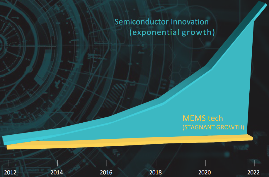
Semiconductor vs. MEMS innovation (Source: Omnitron)
As Eric told me, “We started by talking with Tier 1 suppliers and OEMs and systems integrators asking, ‘What do you need for your scanner?’ and ‘What does it need to be capable of doing?’ One of the first things they’re telling us is that they need a big mirror. They have a beam that needs to go out 200 meters or more, which means they need a mirror that’s bigger than 10 millimeters to address this. There are no MEMS solutions that are anywhere near that size. The biggest ones out there are about five millimeters. The next thing they say is that FMCW is the future of LiDAR, which means they don’t want a mirror that’s resonating, but instead they need to be able to perform step scanning, which means stopping and dwelling while the laser source is emitted and the signal comes back before moving on.”
Eric continued: “When you look at a MEMS mirror, it is essentially a mass on a spring, so it experiences vibrations on the road, and you’ve got to address that. Also, you’ve got to be insensitive to temperature. Depending on where you live, your car can experience tremendous changes in temperature going from your garage to the outside world. These temperature shocks can happen day in and day out, and your LiDAR scanning system needs to be insensitive to this.”
Eric and his colleagues realized that the design rules that were available to build a MEMS mirror lacked the ability for developers to build a solution that really worked for LiDAR, especially the latest and greatest frequency-modulated continuous wave (FMCW) LiDAR, which requires a large mirror that moves quickly and can perform step scanning. So, they decided to go back to the drawing board to figure out what was required to modify and enhance existing MEMS processes. The following diagram captures everything in a crunchy nutshell.
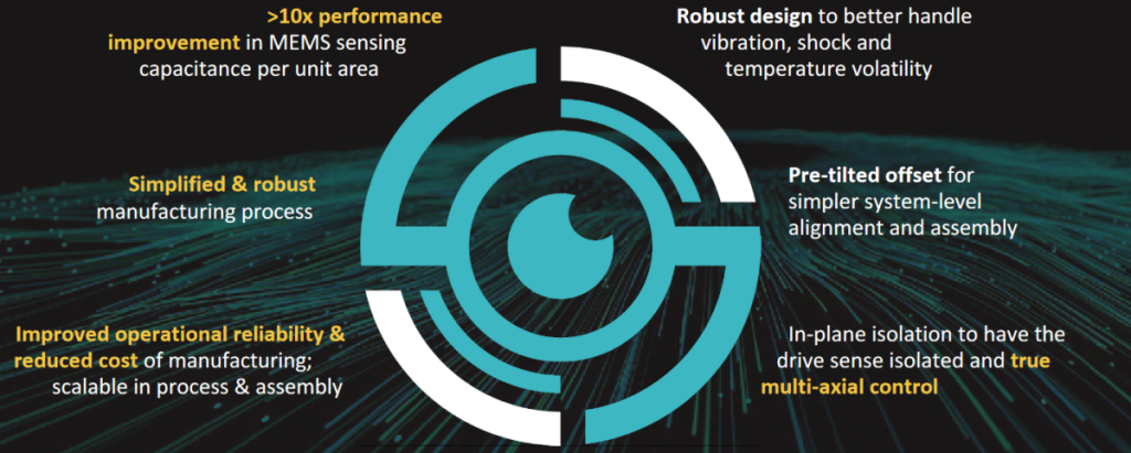
Omnitron’s approach to 3D MEMS design (Source: Omnitron)
The first thing they did was to build a very powerful actuator, which they achieved by improving the capacitance per unit area. In other words, we’re talking about energy density—how much more energy they could pack over a surface area as compared to what’s available in the market. The result is 10 times better than anything else that’s available. Also, they included in-plane isolation to fully decouple any voltage applied to the actuating element from the sensing elements. Even better, they have the ability to implement pre-tilted offsets to the mirrors, which dramatically simplifies system-level alignment and assembly, thereby significantly lowering system cost.
Finally, they have developed a simplified and robust manufacturing process based on existing tools and capabilities that can be found at any industrial foundry. The team developed a clever sequence to achieve this much higher performance while providing great uniformity across the wafer, and they have proved all of this at R&D foundries.
Of course, “The proof of the pudding is in the eating,” as they say, so let’s take a look at the large mirror comparison illustrated in the image below.
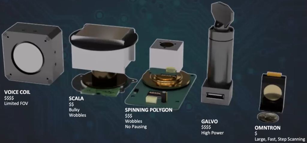
Large mirror comparison (Source: Omnitron)
From left-to-right we have a voice coil-based mirror, which is large (the one shown here has a 20mm diameter) and robust and has a great feedback mechanism. The downside is that it has a limited field of view and costs thousands of dollars.
Going down the line, all of the other existing options exhibit various disadvantages, including high cost, tendency to wobble, no ability to step, or high power. And then we come to the Omnitron mirror on the right. This is large with respect to its mirror (15mm diameter) but not to its overall size, it’s fast and supports step scanning, and it is much more affordable than its legacy competitors.
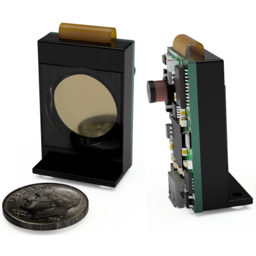
As an FYI, at first, I assumed that the coin lying in front of the Omnitron mirror was a quarter, but I was mistaken because it is in fact a dime.
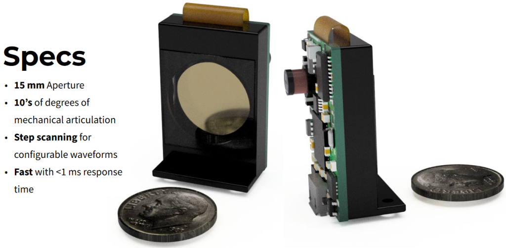
A more detailed look at the Omnitron proof-of-concept (PoC)
(Source: Omnitron)
And, before we bid each other a fond farewell, I’d like to share the following image with you. This data was gleaned from multiple sources, but you can perform a quick cross check by perusing and pondering the Status of the MEMS Industry 2022 report from the Yole Group).
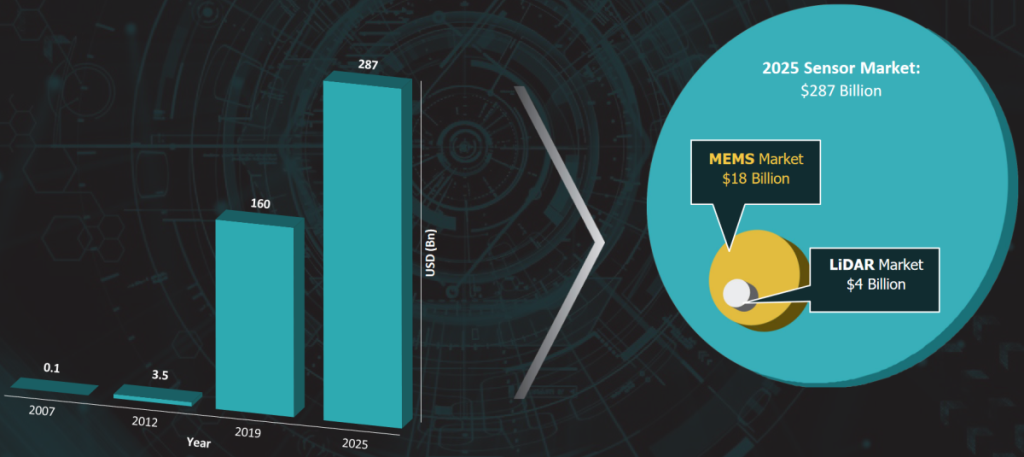
The 2025 sensor, MEMS, and LiDAR markets (Source: Omnitron)
The interesting thing about all of this is that this data does not account for the potential disruption that may be caused by Omnitron’s new patent-pending process. First, the availability of lower-cost, higher-resolution LiDAR sensors could significantly expand the overall LiDAR market. Second, Omnitron’s processes are not only focused (no pun intended) on mirrors, but are instead applicable to MEMS in general, which could dramatically increase the MEMS market as a whole.
As always, we certainly do live in exciting times. I keep on reminding myself that 2025 is now only two years away, at which time we will be a quarter of the way through the 21st century. I don’t know about you, but I’m too young for all this excitement. I think I’ll have to go and lie down. While I do so, I’d love for you to share your thoughts on anything you’ve read here in the comments below.


