


I was just chatting with the chaps and chapesses at Weebit Nano regarding their embedded ReRAM (resistive random-access memory) technology, which may be poised to leap onto the center of the NVM (non-volatile memory) stage accompanied by a frenzied fanfare of flügelhorns.
It probably goes without saying (but I’ll say it anyway) that — like trumpets and cornets — most flügelhorns (Hornbostel–Sachs classification 423.232) are pitched in B-flat, but don’t invite me to start regaling you with any more details about these little scamps, or we’ll be here all day.
The concept of computer memory that can be used to store programs and data is one that has long intrigued me, not least that there’s always something new to be learned. I often ponder what I would do if I were to trip through a time-slip and find myself in the past, in which case building a computer using whatever technology was available to me would always be a possibility.
Just for giggles and grins, let’s take a brief look at the various forms of computer memory that people have employed over the years. We’ll start in the early 1800s (see also my Timeline of Calculators, Computers, and Stuff), when a French silk weaver called Joseph-Marie Jacquard (1752-1834) invented a way of automatically controlling the warp and weft threads on a silk loom by recording patterns of holes in a string of cards. Later, in 1837, the eccentric British mathematician and inventor Charles Babbage (1791-1871) conceived his Analytical Steam Engine. Although it was never finished, this magnificent machine was intended to use loops of Jacquard’s punched cards to control an automatic mechanical calculator, which could make decisions based on the results of previous computations. The Analytical Engine was also intended to employ several features subsequently used in modern computers, including sequential control, branching, and looping.
It wasn’t long until Jacquard’s punched cards were supplanted by a plethora of perforated paper products (try saying that ten times quickly), including punched paper tapes. In 1857, for example, only twenty years after the invention of the telegraph, the British physicist and inventor Sir Charles Wheatstone (1802-1865) introduced the first application of paper tapes as a medium for the preparation, storage, and transmission of data in the form of Morse telegraph messages. In this case, outgoing messages could be prepared off-line on paper tape and transmitted later. (Sir Charles also invented the accordion in 1829, which probably limited his circle of friends.)
In the aftermath of World War II, it was discovered that a full-fledged computer called the Z1 had been built in Germany before the start of the war. The Z1’s creator was the German engineer Konrad Zuse (1910-1995). The amazing thing is that Zuse knew nothing of any related work, including Boolean Algebra and Babbage’s engines, so he invented everything from the ground up. Containing approximately 30,000 components, this purely mechanical computer was incredibly sophisticated for its time. For example, while Zuse’s contemporaries in places like the UK and America were starting to work on machines that performed decimal fixed-point calculations, the Z1 employed a binary floating-point system based on a semi-logarithmic representation. This made it possible to work with very small and very large numbers, thereby making the Z1 suitable for a wide variety of engineering and scientific applications. The Z1 was freely programmable in that it could read an arbitrary sequence of instructions from a punched paper tape. The key point pertaining to our discussions here is that the Z1 boasted a mechanical main memory, which was comprised of 64 words, each containing a 22-bit floating-point value.
Early relay-based computers used relays to implement their memory, which imposed limitations in terms of cost and size. In the case of the Harvard Mark 1 circa the early 1940s, for example, the memory could store 72 numbers, each 23 decimal digits long. Similarly, early vacuum-tube-based computers used tubes to implement their memory, which added the problem of reliability into the mix.
A variety of esoteric memory technologies started to appear around the mid-1940s, including acoustic mercury delay lines, which were formed from thin tubes containing mercury with a quartz crystal mounted at each end. Applying an electric current to a quartz crystal causes it to vibrate. Similarly, vibrating a quartz crystal causes it to generate an electric current. The way in which these delay lines worked was to inject (write) a series of pulses into one end of the tube, read them out of the other end, and feed them back to the beginning. The absence or presence of pulses at specified times represented 0s and 1s, respectively. Although this may seem a tad complicated, 1,000 bits could be stored in a delay line 5 feet long, which provided a much higher memory density than relays or vacuum tubes.
One big problem with delay lines was that they were sequential in nature. This meant you had to wait for the data in which you were interested to pass under your nose (i.e., arrive where it could be accessed). By comparison, in the case of random-access memory (RAM), you can access any data of interest whenever you wish to do so. The predominant form of RAM between 1955 and 1975 was magnetic core store. The idea here was for small donut-shaped beads (cores) formed from a hard ferromagnetic material to be threaded onto thin wires, with three or four wires passing through each core. Pulsing current through the correct combination of wires allowed each core to be magnetized one way or the other, thereby representing a 0 or a 1. Related pulses could be used to read data back out of the store.
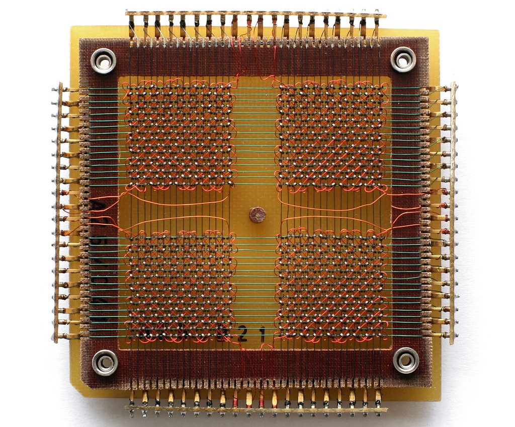
A 32 x 32 core memory plane storing 1024 bits (or 128 bytes) of data. The small black rings at the intersections of the grid wires, organized in four squares, are the ferrite cores (Image source: Konstantin Lanzet/Wikipedia)
The great thing about magnetic core memory was that it was non-volatile, which means it remembered its contents when power was removed from the system. The bad news was that it employed a “destructive read,” which meant that reading a word caused all of the bits in that word to be set to 0. Thus, the associated controller had to ensure that every read was immediately followed by a write to re-load the selected word.
Another interesting memory implementation based on magnetism was bubble memory, which appeared on the scene in the late 1960s and early 1970s. In this case, a thin film of a magnetic material was used to hold small, magnetized areas, known as bubbles or domains, each storing one bit of data. Looking back, it’s funny to recall that — based on its capacity and performance — many people in the 1970s promoted bubble memory as a contender for a “universal memory” that could be used to satisfy all storage needs (the reason I say this is funny is that we are still searching for that elusive “universal memory” to this day).
And then, of course, we started to see the introduction of semiconductor memories. The first such memories were created out of discrete bipolar junction transistors by Texas Instruments in the early 1960s. These were followed by non-volatile memory integrated circuits (ICs) in the form of mask-programmed read-only memories (ROMs), PROMs, EPROMs, EEPROMs, and Flash, along with volatile memory ICs such as static RAMs (SRAMs) and dynamic RAMs (DRAMs).
Each type of memory has its own advantages and disadvantages, which means systems usually feature a mélange of memories. In the case of a typical personal computer, for example, the CPU will contain a relatively small amount (a few megabytes) of very-high-speed, high-power SRAM forming its cache, while the motherboard will include a relatively large amount (say 8 or 16 gigabytes) of relatively high-speed, high-capacity, low-power DRAM (in one form or another). Meanwhile, the bulk storage might be provided by a solid-state drive (SSD) in the form of Flash memory.
Similarly, a typical microcontroller unit (MCU) might contain a mix of Flash, SRAM, and EEPROM. The non-volatile Flash with a limited endurance (number of write cycles) is used to store the program, while the volatile SRAM with an essentially unlimited endurance is where the program creates, stores, and manipulates variables when it runs. The problem with the Flash is that you have to erase thousands of bytes at a time in order to write new data. This isn’t an issue if you are loading an entire new program, but it’s a pain in the nether regions if you wish to store only a few bytes of data. Thus, the MCU will also include a small amount (perhaps a couple of kilobytes) of non-volatile EEPROM (electrically erasable programmable read-only memory) in which we can store modest quantities of long-term information, like configuration settings or occasional sensor readings, for example.
Now, when it comes to embedded NVM, Flash is wonderful — it’s certainly changed my world for the better — but it’s not the only game in town. Other NVM contenders include magnetoresistive RAM (MRAM), which stores data in magnetic domains, and phase-change memory (PCM or PCRAM), which stores data by changing between amorphous and crystalline states.
Yet another NVM possibility — and the reason I’m writing this column — is resistive RAM (ReRAM), which stores data by changing the resistance across a dielectric solid-state material. And, of course, ReRAM is Weebit Nano‘s “claim-to-fame,” as it were. Let’s consider a simple 1T1R (one transistor, one resistor) ReRam cell structure as illustrated below:
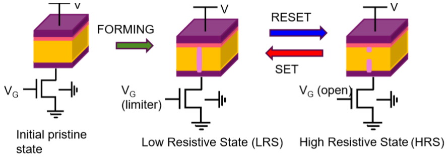
ReRAM basic operation (Image source: Weebit Nano)
Note that the transistor will be created in the silicon along with all of the other transistors forming the device. Meanwhile, the resistive part of the cell will be constructed between any two adjacent metallization layers. When the device is created, the cell is in its initial pristine state, with (essentially) infinite resistance. Setting the cell involves the creation of a conductive filament (CF), which places the cell in a low resistive state (LRS) with a resistance <10 kΩ representing a logic 1. Resetting (erasing) the cell causes partial dissolution of the CF, thereby placing the cell in a high resistive state (HRS) with a resistance >1 MΩ representing a logic 1.
Remember that we’re talking about embedded NVM here — that is, having the NVM created as part of a device like an MCU — not bulk NVM like the discrete Flash devices used in an SSD. The reason this is important is that embedded Flash is beginning to have problems scaling below the 40 nm process node, while ReRAM is happy to keep on going to 28 nm and below (I’m informed that there’s a direct roadmap down to 10 nm).
Take a look at the following comparison chart showing Weebit Nano’s ReRAM versus PCM, MRAM, and Embedded Flash technologies (data sources are Global Foundries, TSMC, Yole, and company data).
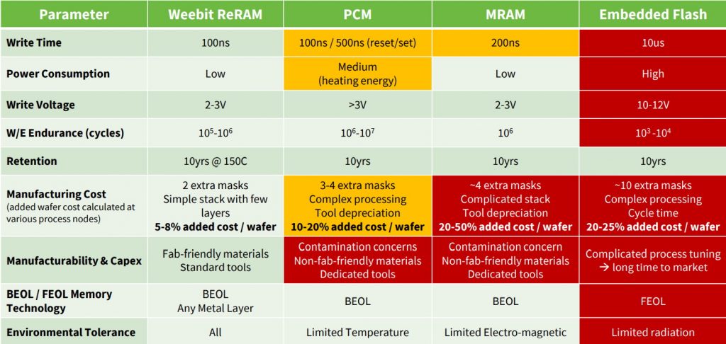
Weebit Nano’s ReRAM versus PCM, MRAM, and Embedded Flash technologies (Image source: Weebit Nano)
Some key features that immediately catch one’s eye are that embedded Flash requires a write voltage of around 10 to 12 volts, has a write time of around 10 µs, and is not bit/byte addressable. By comparison, ReRAM requires a write voltage of only 2 to 3 volts (the read voltage is only 0.5 volts), has a write time of 100 ns, and is bit/byte addressable. When it comes to accessing data, ReRam has a read time of 10 ns, while embedded Flash has a read time of 20 ns. Also, while embedded Flash has an endurance of 103 to 104 write/erase endurance cycles, ReRAM boosts this to 105 to 106 cycles, coupled with a retention of 10 years at 150°C, which isn’t too shabby, let me tell you.
Another point that may be of interest for certain applications is that — due to elements like its charge pumps — embedded Flash takes some time to “wake up” from a deep sleep mode. By comparison, ReRam is effectively “instant-on.”
Also, adding embedded Flash to a device requires around 10 extra mask steps and — due to its floating gates — involves changes to the front-end-of-line (FEOL) processes where the individual devices (transistors, capacitors, resistors, etc.) are patterned into the semiconductor. As a result, including embedded Flash adds about 20% to 25% to the cost of the wafer. By comparison, Weebit Nano’s ReREM requires only two additional mask steps using fab-friendly materials and standard tools, and these steps take place as part of the back-end-of-line (BEOL) processes when the metallization layers are added. As a result, using ReRAM adds only 5% to 8% to the cost of the wafer.
Last, but certainly not least, another item that caught my attention was the “Environmental Tolerance” line in the table, where we see that PCM has limited tolerance to temperature, MRAM has limited tolerance to electromagnetic noise, and Flash has limited tolerance to radiation effects. By comparison, ReRAM has tolerance to all of these environmental conditions. (I wonder what the creators of the early computers would have thought if we could go back in time and tell them about ReRAM technology.)
“But is all this real, or is it just ‘pie in the sky’?” I hear you cry. Well, the guys and gals at Weebit Nano recently announced that they’ve completed the design and verification stages of an embedded ReRAM module — which includes a 128Kb ReRAM array, control logic, decoders, IOs (Input/Output communication elements) and error-correcting code (ECC) — and taped-out (released to manufacturing) a test-chip that integrates this module. This test-chip — which also includes a RISC-V MCU, SRAM, system interfaces, and peripherals — will be used as the final platform for testing and qualification, ahead of customer production.
So, when will folks be able to start embedding Weebit Nano’s ReRAM modules in their MCUs and SoCs? I’m guessing sometime in 2022, which means that — if you are interested in taking a deeper dive into this technology — now would be a great time to contact the folks at Weebit Nano to start the ball rolling (if you do call them, tell them “Max says Hi!”). In the meantime, are there any other memory technologies — from the past, present, or (potentially) future — that you think I should have mentioned in this column?


Hi Max, great article. In my early days I worked on test systems for core memory airborne systems, 4K x 8 bits. It was fun writing various worst-case data patterns to a core plane and reading them back to an oscilloscope and test rig to verify the patterns. Later in life the PC based control systems that I installed at GM Powertrain required nonvolatile memory for retention of data and certain variable states but not the program which was loaded from disc. A battery and CMOS memory did the trick for these 2K plug-in PC cards. People howled about using a PC and disk memory on the factory floor but both turned out to be reliable. This whole experience got me thinking about synthesizing directly to hardware and eliminating the need for the disk memory, i.e. program memory. That thinking resulted in a patent for what is described as a ‘Flowpro Machine’. So, is eliminating the need for program memory (potentially) a future memory issue? Perhaps it’s time for an article on hardware synthesis and the ramification to memory systems.
Please help me understand the feasibility of this memory. Let’s consider one bit (1T1R) in the best case scenario: V=2V (from 2-3V) specified and LRS = 10k (specified <10k). The power dissipated on this 1 bit of memory is: V^2/LRS = 4/10k =0.4mW. So, the tested version of "128Kb ReRAM", in the case of equal "ones" and "zeroes", would dissipate 64kb * 0.4mW = 25.6W, which will require a huge heatsink. IMHO, it is not going to be practical.
Am I missing something?
Thanks.
Victor Kolesnichenko
victork@ca-cosnulting.us
Victor perhaps I have missed something. For your dissipation calculation what do you consider the system word length is and the read time per word. You appear to be suggesting the whole 128kbit memory is read at one instant in time and you calculation is for instantaneous power. A more reasonable calculation would be average power. This is an NV memory and most of the memory work will be done by the associated SRAM and processor.
The data on MRAM is not accurate. Our Numem NuRAM the following characteristics:
– Write time: 35ns (including time for overhead processing to preserve endurance and verify results)
– Write Voltage: much lower than indicated
– Write Endurance: much higher than indicated
– while not indicated here, Read time on NuRAM is 5ns which i believe is faster than what is achieved today on RRAM.
– Faster Read/Write means proportionally lower Dynamic Power (2x faster speed means 2x lower power) as these are non-volatile so they are shut down post Read/Write
– Leading Foundries have 3 additional mask layers not 4. Premium for eMRAM, is higher than RRAM but cost delta is much lower. Pricing, of course, mostly depends on Foundries’ pricing strategy.
So the tradeoff is some cost reduction versus lower power/ higher performance.
In addition to the mercury delay line, there is also a “solid state” version. The mercury delay line is replaced with a steel wire in a spiral pattern, with transducers on both ends. An acoustic pulse emitted from one end of the wire can be picked at the other end, similar to the mercury delay line. I think the capacity is a couple of thousand bits. The whole device is placed inside an enclosure the size of a thick 8″ floppy disk (remember those?). I still have one of these that I bought from a surplus house many years ago. The same vendor also had magnetic drum memory used on some military aircraft.