


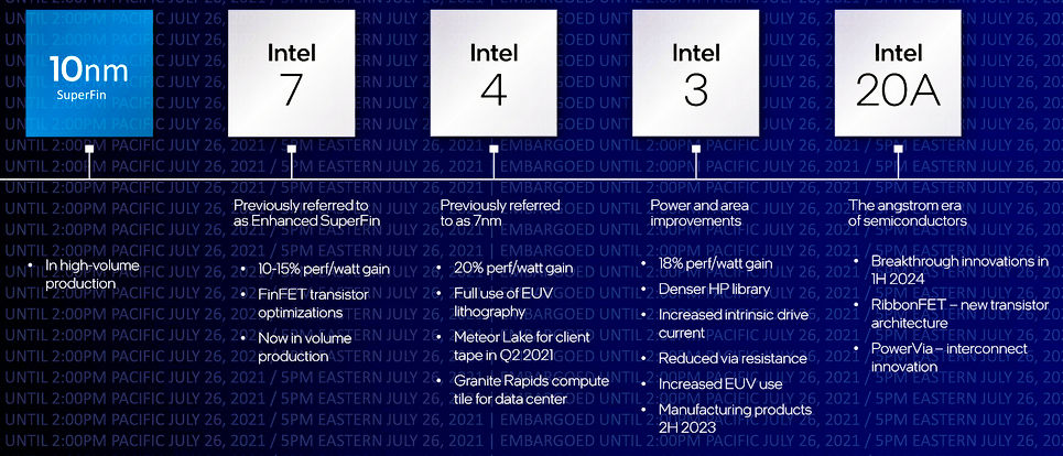
Intel took a lot of flak when it announced new names for its future semiconductor process nodes during the Intel Accelerated event in Late July. The new nodes are called Intel 7, 4, 3, and 20A. Industry pundits have knocked the company for calling its 10nm enhanced SuperFin process node “Intel 7.” (Intel announced and demonstrated 12th Generation i5, i7, and i9 Core processors built using the Intel 7 process node just last week at its Intel InnovatiON developer event, so this process technology is clearly well in hand.) The company now uses the name “Intel 4” for the node previously called 7nm. Intel 3 and Intel 20A are all-new node names. Part of this node renaming has roots in marketing, and part is simply facing reality.
Intel has renamed its upcoming process nodes to conform to industry conventions rather than its own perception of reality
In the past, Intel had said that its 10nm enhanced SuperFin node (now renamed Intel 7) was roughly equivalent in power and performance to TSMC’s 7nm node. Confusing, no? The company has also stated that industry analysts have asked Intel to update its process node nomenclature to reflect the company’s true competitive position in the semiconductor process arena. All of that is the marketing part of the renamed nodes.
The reality part is this: the nanometer nomenclature hasn’t been accurate for a long, long time. Not for Intel and certainly not for any other silicon foundry. This situation is like the scoring system in the hit comedy television show “Whose Line is it Anyway?” The points don’t matter.
Years ago, process node naming was based on a transistor’s smallest feature size. That naming convention was specifically developed for a planar MOS transistor, and the smallest transistor feature was invariably the transistor’s gate length. That naming convention went out the window when FinFETs took over from planar MOS transistors, and all vendors’ process node names became nothing more than estimated equivalents for the power and speed you’d get from an equivalent planar MOS transistor. Except that they couldn’t actually make those planar MOS transistors any more. Planar transistor technology gave out. MOS transistors just don’t work well at current lithographic levels. That’s why we turned to FinFETs. Intel introduced its first FinFET process at the 22nm node – way back in 2011.
RibbonFETs and angstroms
Ten years later, the fundamental structure of transistors is about to change yet again.
FinFET gates are driven from three sides. That’s two more sides than are driven in planar MOS transistors, which results in much better transistor performance at the expense of more complex manufacturing techniques. However, driving three sides of the FinFET transistor’s gate no longer achieves the desired speeds and leakage currents. We must now drive all four sides of the gate. These 4-sided gate-drive structures are universally called “gate all around” or GAA.
Universally, except for Intel, which calls its GAA transistors “RibbonFETs,” which are currently scheduled to appear in the Intel 20A process that’s due to appear in the first half of 2024 (barring delays). Notice the “A” in the process name. “A” is for “angstrom.” Instead of calling this process node “Intel 2” as with the previous process nodes, Intel switched units from nanometers to angstroms. An angstrom is 10-10 m, or one tenth of a nanometer. I think we’re supposed to simply disregard the fact that Intel dropped the “nm” from the bigger process nodes.
Presumably, this nomenclature change to angstroms allows for fractional nanometer node naming. That’s similar to the situation we had with the previously used unit, microns. Back in the dark ages, we had 3, 2.5, 2, 1.5, 1.3, 1.2, and then 1 micron process steps, followed by 0.8, 0.75, 0.7, 0.5, and all the way down to around 0.25 microns. Somewhere around that point, we jumped from microns to nanometers. Based on my best recollection, that nomenclature change occurred at 0.18 microns, which was popularly called 180 nm. When was that? Around 1998. More than two decades ago.
That means the nanometer process node ruler will have been used for almost a quarter of a century when the angstrom era starts. The Intel angstrom nomenclature allows the company to have process nodes named Intel 18A, Intel 17A, Intel 16A, and so on. That sounds so much better than Intel 1.8, Intel 1.7, Intel 1.6, and so on, doesn’t it? Sounds like they’re making more progress this way, right? However, the progress from one node to the next isn’t nearly as big as it once was. From the image above, you can see performance/watt improvements of between 10 and 20 percent from one Intel process node to the next, and the image doesn’t even discuss density improvements.
Moore’s Law lies a moldering in the grave
And that gets us to the meat of the matter for this article. Based on all that’s written above, I have very sad news for you. Moore’s Law is dead, despite Intel CEO Pat Gelsinger’s bold and enthusiastic promise to meet or beat Moore’s Law every year for the next 10 years, made last week during the Intel InnovatiON event. Scaling a process node by shaving a few angstroms from one generation to the next does not achieve a doubling of transistor density, and that is the true essence of Moore’s Law.
From my perspective, there’s a lot of confusion surrounding Moore’s Law. First, Moore’s Law has long been too closely intertwined and confused with Dennard Scaling, which says that planar MOSFET speed and power scale down proportionally as transistor density goes up. In the early days of semiconductors, when a new process technology shrank transistor area by 50%, the transistor’s speed would double and power would halve. We got half-sized transistors with twice the speed that ran at half the power with each new process node, every couple of years. Those were indeed very good times, and Moore’s Law was in full sway. However, Dennard Scaling was an observation specifically for planar MOS transistors, and we haven’t been making that kind of transistor using the most advanced, new process nodes for about a decade.
Moore’s Law did not refer to transistor power or speed. Moore’s Law says that the number of transistors on a chip doubles approximately every two years. That’s all it says. You can look it up if you like. Gordon Moore’s original article in Electronics magazine from April 19, 1965 was titled “Cramming more components onto integrated circuits.” It’s conveniently posted on Intel’s Web site for you to read. This article appeared three years before Moore and Bob Noyce founded Intel, while Moore and Noyce were both still working for Fairchild Semiconductor.
Moore performed an unbelievable feat of prognostication in his groundbreaking article. The semiconductor industry eventually embraced and transformed his prediction into a self-fulfilling prophecy, which was based on a very few data points. The first data point was a single transistor. The second data point was one of the first commercial integrated circuits, a 3-input NOR gate called a Fairchild μLogic Type G RTL chip.
According to Dr. David Patterson, Moore’s Law lasted through 2015 when it ran out of gas. (See “Fifty (or Sixty) Years of Processor Development…for This?”) How could Patterson say that Moore’s Law died in 2015 when Intel’s executives would uniformly have you believe that Moore’s Law is alive and well today? It’s because of a phrase on page 2 of Moore’s 1965 paper. That phrase is: “…the production of larger and larger circuit functions on a single semiconductor substrate.” (Emphasis is mine.) Moore’s Law is about monolithic integrated circuits, and that’s just not where the semiconductor industry is heading.
In fact, on the 50th anniversary of the International Solid State Circuits Conference, in 2003, during a presentation titled “No Exponential is Forever,” Gordon Moore himself stated categorically that “…no physical quantity can continue to change exponentially forever.” Moore’s Law was already dying nearly two decades ago, and Moore saw it himself.
My current poster child for signaling the end of Moore’s Law isLaw’s is Intel’s own Ponte Vecchio GPU. Intel is assembling this integrated device using 47 active “tiles” – Intel’s name for the chiplets or die in a multi-chip package – manufactured by multiple semiconductor vendors from five different semiconductor process nodes, all combined in one package using 2.5D and 3D assembly techniques to produce an integrated product with more than 100 billion transistors. (Please be sure to read that last sentence with a Carl Sagan accent and emphasis on “billion.”)
Some people have claimed that Moore foresaw multichip packaging in his article. They cite this phrase:
“It may prove to be more economical to build large systems out of smaller functions…”
But they seem to omit the second half of this sentence:
“…which are separately packaged and interconnected.”
Here, Moore was clearly discussing the use of multiple individually packaged chips on one board, a staple of board-level design since integrated circuits first appeared in the 1960s. From my perspective, Moore was clearly not predicting today’s multichip packaging with this sentence. In fact, his article discusses the possibility that monolithic ICs with 65,000 components per IC could appear in 10 years, by 1975, which was far more discrete components than any single printed circuit board could accommodate back in 1965 when Moore’s article appeared. Who could possibly need more than 65,000 components? If Moore thought about it at all back then, and he probably did, he must have seen that multichip packaging technology would not be needed until far, far in the future. Well, that future has arrived.
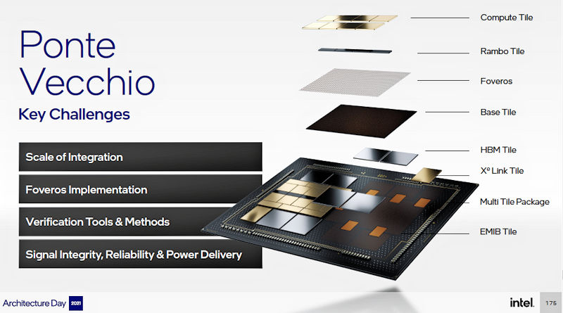
Intel’s Ponte Vecchio GPU incorporatesincorporate 47 tiles from five different process nodes to cram 100 billion transistors into one package. (Image Credit: Intel)
Multichip packaging makes sense only because different process nodes deliver different cost/performance/capabilities tradeoffs, because we’re at the reticle limits of current chip-making equipment, and because 2.5D and 3D packaging techniques are now sufficiently practical and economical to make this approach work commercially. Why shouldn’t blocks and subsystems be made from the most efficient semiconductor process node possible, assuming you have the manufacturing processes needed to assemble all of these tiles or chiplets reliably and economically? Ponte Vecchio is admittedly an engineering marvel, but it’s most definitely not a monolithic chip, and so it’s not an example of the original Moore’s Law in action.
Except for the massively mythological underpinnings of Moore’s Law, it’s really not important to most of us how Intel crams 100 billion transistors into the Ponte Vecchio package. It’s not important to systems engineers using Ponte Vecchio GPUs in their designs. It’s not important to people using graphics software or computer games that run on Ponte Vecchio GPUs. The device’s performance, power, and price (the three fundamental “P”s of all engineering design) are what’s important to those of us who live outside of the package.
Intel plans to build Sapphire Rapids, the code name for the company’s next-generation Xeon processor, in a similar manner. Intel will manufacture Sapphire Rapids using four CPU tiles and 2.5D assembly based on the company’s EMIB (Embedded Multi-die Interconnect Bridge) technology. Versions of the Sapphire Rapids processor will also incorporate multiple HBM2 (High Bandwidth Memory 2) DRAM stacks in the same package.
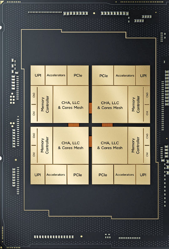
Intel’s Sapphire Rapids, the next-generation Xeon CPU, will incorporate four CPU tiles linked by four EMIB bridges. (Image Credit: Intel)
Multichip packaging is not unique to Intel. Far from it. AMD, Nvidia, and Xilinx all manufacture integrated devices that look like monolithic integrated circuits on the outside but are multichip devices – interconnected collections of tiles or chiplets – on the inside. (Actually, these fabless semiconductor vendors all have their devices manufactured and packaged for them by 3rd-party foundries – often that’s TSMC.) This has been the situation for more than a decade.
For example, Xilinx introduced the Virtex-7 2000T FPGA in 2011. It’s based on a multichip package that puts four FPGA dies on top of one silicon interposer. TSMC fabricates that device for Xilinx. Around the same time, multichip packaging allowed Xilinx to incorporate 28 Gbps transceivers into its Virtex-7 580T FPGA before it was possible to build these transceivers directly into the CMOS FPGA die. Xilinx has expanded its use of multichip packaging with each new FPGA generation. That’s a good indication that multichip packaging works well, at least for the high end of the IC market.
So, welcome to the angstrom era. It’s a “Beyond Moore” era. Now freed of the emotional and economic need to put everything onto one die, this new era of semiconductor manufacturing is already producing bigger and better integrated devices than ever before. It just won’t deliver these goodies by relying solely on monolithic ICs and Moore’s Law.
Moore’s Law may be dead, but the spirit of Moore’s Law endures. Just ask Pat Gelsinger.
For more fascinating details on the origins of Moore’s Law, see “Moore’s Law and the Seven Devices.”


Two comments:
Re: “The company has also stated that industry analysts have asked Intel to update its process node nomenclature to reflect the company’s true competitive position in the semiconductor process arena.”
One of those analysts was EE Journal: https://www.eejournal.com/article/no-more-nanometers/
Re: “Moore’s Law says that the number of transistors on a chip doubles approximately every two years. That’s all it says.”
The 1965 “Cramming More Components…” article actually said it would double every YEAR. “The complexity for minimum component costs has increased at a rate of roughly a factor of two per year … Certainly over the short term this rate can be expected to continue, if not to increase. Over the
longer term, the rate of increase is a bit more uncertain, although there is no reason to believe it will not remain nearly constant for at least 10 years.”
Moore revised his forecast ten years later, in 1975 – to a doubling every two years. That was also about the time Carver Meade started promoting the label “Moore’s Law” for the prediction.
This is another case of “Look Ma, what I can do!” as opposed to what I should do.
It is absurd to think that mere humans can even conceive of a design that can use that many transistors.
OR that design timing closure and verification is possible on such a massive scale.
OR that the pitiful HDL Tools can begin to handle so many gates.
OR that it is possible to get enough data on and off chip at the necessary speed.
OR that it is possible to define the interconnection of that many gates.
Whether or not Moore’s Law exists is mute, because there is a severe chip shortage.
It is time for a new approach to design entry and a methodology that works for heterogeneous design.
Has anyone heard of the M1 chip?