

As if it weren’t already complex enough, x86 processors from Intel and AMD allow you to make software and memory even more indirect and complicated. This week we dive into virtual memory, demand paging, and other advanced features that x86, ARM, RISC-V, and most other modern CPUs all implement but that aren’t well understood.
What the heck is virtual memory? It can mean a couple of different things, but usually it means you’re pretending that your system has more memory than it actually does. You’re faking out your processor and lying to your programmers to make them both think that there’s lots of memory where there really isn’t. The idea is to make the imaginary memory look and act virtually the same as real memory, hence the term.
Sometimes you can use a hard disk drive (HDD) or solid-state disk (SSD) as ersatz memory, and this trick is called demand paging. Other times, you just want to make the memory you have appear like it’s at a different address, a trick known as address translation. Finally, some processors can enforce privilege protection on designated areas of memory; x86 programmers call this page-level protection.
Let’s start with address translation. It’s the easiest of these techniques to wrap your head around and also the most useful. In the x86 world, memory addresses are already complicated. An address pointer held in a register like EAX or ESI isn’t the real memory address because x86 processors all use memory segmentation. That “address” is really just an offset into a segment of memory, which might start at almost any arbitrary base address. So, the real address is the sum of the segment’s base address plus the offset address you started with. Okay so far?
Intel’s documentation calls the address in your register the logical address and the resulting segment-plus-offset the linear address. Normally, that’s as far as it goes. But when you enable virtual memory addressing (it’s off by default), you tack on yet another level of indirection: the physical address.
You’ll recall that converting logical addresses to linear addresses involves creating a bunch of tables in memory. Guess what – converting linear addresses to physical addresses works the same way! You get to create a whole new set of tables in memory that manipulate every memory address yet again. Why add yet another level of indirection, more tables, and more complication? Because sometimes we want to hide the actual physical hardware implementation from programmers – even low-level OS and driver programmers. Sometimes you want to fool even the CPU into believing that there’s memory where there really isn’t.
The figure below illustrates how this works. And yes, it adds not one, not two, but three new tables in memory, all of which you get to create. Starting with the familiar linear address at the top (in blue), this would normally be where your journey ends were it not for virtual memory. Instead, the 10 most significant bits are used as an index into the first table, called the page directory. The data it finds there will point to a second table, called the page table. This is just one of potentially 1024 different such tables, but for clarity, we’ve illustrated only this one.
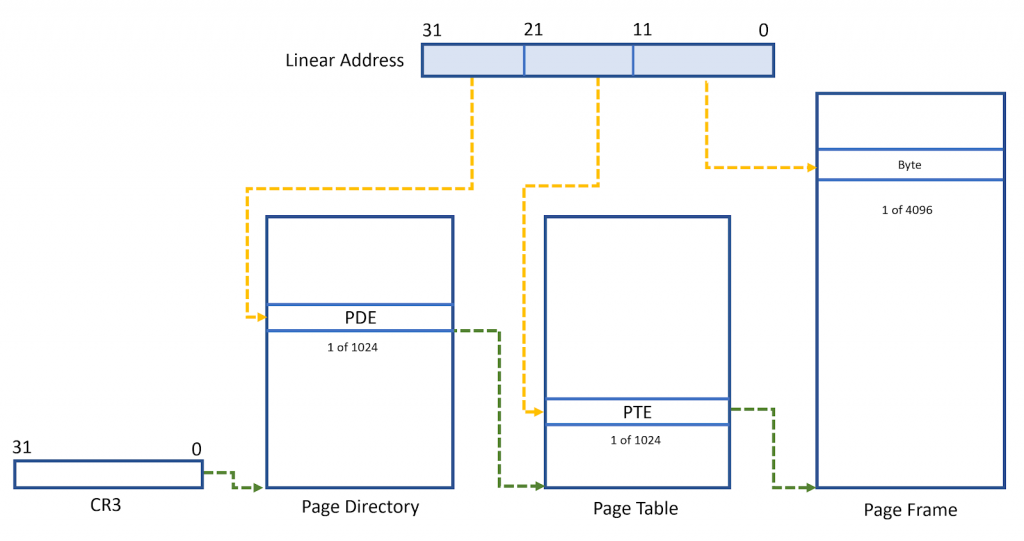
The ten next-most-significant bits (bits 12–21) in your linear address are used as an index into the page table, and the data it finds there will point to an address in actual physical memory. This is what your system’s hardware will see. In fact, it’s the only address your hardware will see. The logical and linear addresses leading up to this are merely fictional software constructs.
Finally, the lower 12 bits in your address select the actual byte address within a physical memory, as shown.
Whew! That’s a lot of indirection and tables within tables. It’s all the more impressive (or terrifying) when you realize that every single access to memory – reads, writes, code fetches, stack push/pop, all of it – has to go through every one of these steps. How can the processor possibly keep up? And wouldn’t every memory access trigger an even greater number of these table lookups? That seems crazy.
The good news is, your processor caches copies of some (but not all) of these table entries for quick access. Most programs exhibit locality of reference, meaning their code is all in one place and their data is stored in one place. That’s helpful because it means the processor will be looking up the same page table entries over and over again without a lot of random jumping around. By caching copies of those recently used pieces, the subsequent lookups go very quickly.
The process of cracking your linear address apart into thirds and looking up each entry in the tables is called a table walk. Table walks can be very time-consuming, but that’s what the cache is for.
More scary stuff: the page directory has 1024 page directory entries (PDEs), meaning it points to 1024 different page tables, and each page table also has 1024 entries. At 4 bytes per page table entry (PTE), that’s 4KB per page table, or 4MB for a full set of page tables. Fortunately, that’s not really required.
The page tables come into play only after the processor translates a linear address into a logical address. So, if your code never accesses a certain range of addresses, there’s no need to set up the tables to translate those addresses. It’s a rare program that actually uses the whole 4GB linear address space of the processor, so you can probably omit the page tables for most of that 4GB space.
You can even trim off part of the page directory if you’re clever and you know that software is limited to low addresses. For example, if you know that no program will ever generate an address above, say, 0x00480000, you need only two entries in the page directory (PDE0 and PDE1); all the others can be left undefined. You’ll need to create only two page tables, too. Technically, an x86 processor will think the entire page directory is still there, but if the CPU never tries to access it, it won’t matter.
Why would you ever want to go through all this address translation rigamarole? What do you gain by it? One big benefit is to make your scattered physical RAM and ROM look like it’s all in one contiguous block. It’s easier for programmers to access memory if they believe (erroneously) that it can all be found at consecutive addresses, with no holes or weird alignment issues. It’s a pain to break up data arrays (or worse, code) into pieces that fit into physical memory. With address translation, you don’t have to. All memory appears contiguous, even if it’s not. Even your operating system won’t know the difference.
Another use is aliasing. With page tables, you can make the same physical memory appear at two (or more) different linear addresses. A particular ROM, for instance, might be readable at 0x00000000 and at 0xFF003400. This would give every byte in that physical space two linear addresses. Same goes for RAM space. This might be handy if you’ve got programs with hard-coded addresses that you can’t change. Simply map the addresses they want to the memory you’ve got.
That covers the basics of address translation. Next, we’ll look at demand paging, page-level protection, and some code samples that make this all work.


