


Part 2 of this article series discussed the development of the first successful programmable logic device, the Signetics 82S100 FPLA (field programmable logic array). A Signetics salesperson tried to convince John Birkner, a minicomputer designer at Computer Automation in Irvine, California, to use the 82S100 in his designs, but Birkner saw that the device was too costly, too big, and too slow. He thought he should go to Silicon Valley to set the IC vendors straight.
John Birkner soon got the chance to “go up there and tell them what they need.” Feeling the need for a job change, Birkner rented a janky Cessna 180 and flew himself up from Irvine to San Jose, California where he interviewed with AMD and MMI. The plane lost oil during the entire trip and Birkner had to land and refill the oil cooler a few times, but he made it to San Jose. Barely. Both companies made offers. Birkner chose MMI.
Eventually, Birkner’s boss at MMI, Clive Ghest, asked Birkner to consider how MMI could harness its titanium-tungsten fuse technology, used in the company’s PROMs, to make FPLAs. (MMI attempted to become a second source for the Signetics 82S100 FPLA, but MMI’s titanium-tungsten fuses would not work with the 82S100’s mask-level design because they exhibited much higher resistance than the nichrome fuses that Signetics used. They could not be blown open by the available programming voltages.)
In his oral history, Birkner explains his thought process after Ghest’s request:
“…that’s when the wheels started to turn. Taking all my experience designing TTL, having the 7400 gold book of TTL [from Texas Instruments] – a few hundred different components all memorized in my head – because we had to work out those puzzles on the PC board – how do we cram – how do we do Boolean minimization when you really can’t minimize?
“You’ve just got these chips that are already preconfigured. You’ve got … four two-input NANDs, or two four-input ANDs. Or they’ve got some ORs. And you really couldn’t minimize, except with your brain, your head, to minimize the number of chips on the board.
“It just struck me one day, this whole book of 7400 TTL combinational and sequential circuits could be put in a few chips. It just struck me. All these AND gates and OR gates, they can just be crammed into this PLA.
“Well, I already had the concept that a PLA could do that. But I have never been given the task of, well, what would be a good product that computer designers would use? So I was fresh from being a computer designer knowing the needs of space, and cost, and performance. And also now knowing PROMs, knowing the architecture of the PROMs… I drew the architectures of a PROM. And I drew the architecture of an FPLA. And I drew all the little fuses. I used X’s for all the little connections. And you look at those two architectures… the cost of this was too much. The performance was too low.
“What if I just took this PROM and flipped it? I made the AND-array be the OR-array, and the OR-array be the AND-array. It was kind of a hybrid between these two architectures. And I drew this new PAL architecture in the center… And that really gelled with people who wanted to understand. They could see the PROM architecture. They could see the FPLA architecture, and they could see this new thing!
“And this new thing was fast, cheap and small.”
Birkner had realized that he could toss out some of the FPLA’s programmable capabilities, and with a programmable AND array and a fixed OR array that combined all of the AND terms, he’d get a chip that could do most of what the FPLA could do, but it would be faster and cheaper. With a little extra work by the logic designer, PALs could be made to do almost anything that an FPLA could do, but faster, with less power consumption, and at lower cost. That’s exactly the kind of engineering tradeoff that designers lust to make. They feel smart when they successfully move in the right direction along all three dimensions of the price/power/performance (PPP) curve.
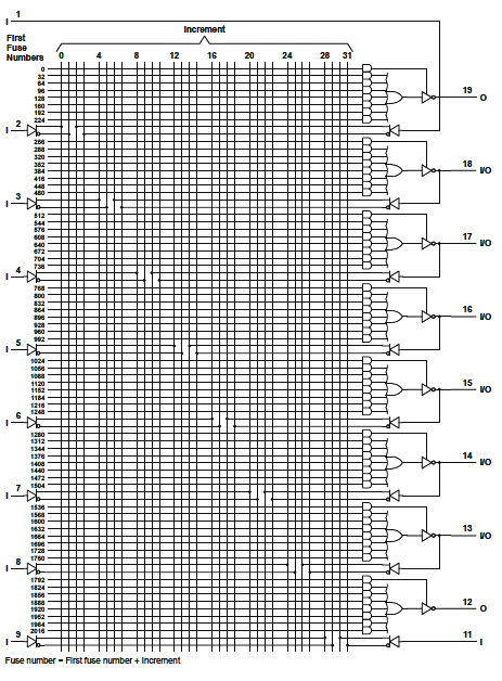
A schematic diagram of an MMI 16L8 PAL appears below. As with the 82S100 FPLA (see Part 2 of this article series), the PAL has a fuse at every row and column intersection that does not appear on the schematic. Also like the 82S100, the unneeded fuses are all blown open during programming:
MMI introduced the first members of its new PAL family in March, 1978, in a 2-page ad in Electronic Design magazine. Family members featured different mixes of inputs and outputs, with and without output registers or latches. MMI packaged all of the initial PAL family devices in 20-pin skinny plastic DIPs, as shown in the image below.
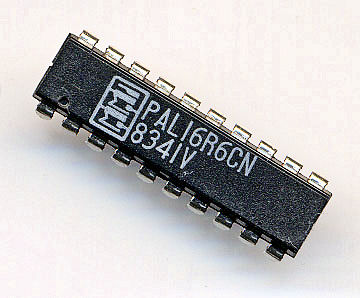 MMI packaged all of the initial PAL family devices in 20-pin skinny plastic DIPs. Photo Credit: Michael Holly
PALs became wildly popular, quickly, for all the reasons that Birkner had foreseen. They were fast enough to replace a couple of layers of TTL gates directly. Power consumption was low enough to not be a problem. And the cost, while not as low as MMI had wanted, was low enough to give design engineers only a momentary pause when deciding to use them.
Perhaps the biggest advantage that PALs offered could not be found on the PPP engineering curve. PALs reduced design risk by allowing a design to defer part of a design until later in the project. By dropping a PAL into a design when requirements weren’t clear or when other forms of design uncertainty crept in, the design decisions for that portion of the circuit could be postponed until long after the circuit board was fabricated.
When the boards came back from the pcb shop and debugging began, engineers could develop design changes to fix bugs in minutes, simply by blowing a new PAL and plugging it into the board. Of course, successfully using this feature depends on the design engineer’s skill in predicting where design bugs might show up. That’s where you wanted to drop a PAL into the circuit.
This “feature” might not seem like much of an advantage today, when a circuit board design can be sent to a pcb fabricator over the Internet instantly, and a fabricated board can arrive as early as the next day, but in the late 1970s and early 1980s, board fabrication took weeks, not a day or two. So dropping a PAL into the design provided weeks of breathing room on finalizing design requirements for the portion of the design that would fit into the PAL. Designers used this feature to their advantage, a lot (I did), and grew to depend on PALs for added insurance against design risks.
Birkner also devoted a lot of effort to marketing PALs. In his oral history, he especially notes the work that went into the development of MMI’s PAL handbook, which was the primary marketing tool for PALs at the time. Here’s how the handbook described MMI’s PALs (Note: gender-specific pronouns from the era have been preserved, intentionally. It’s history from the 1970s, folks! I’m recounting it, not rewriting it.):
“The PAL is an extension of the fusible link technology pioneered by Monolithic Memories for use in bi-polar PROMs. The fusible link PROM first gave the digital systems designer the power to “write on silicon.” In a few seconds he was able to transform a blank PROM from a general purpose device into one containing a custom algorithm, microprogram, or Boolean transfer function. This opened up new horizons for the use of PROMs in computer control stores, character generators, data storage tables and many other applications. The wide acceptance of this technology is clearly demonstrated by today’s multi-million dollar PROM market.
“The key to the PROM’s success is that it allows the designer to quickly and easily customize the chip to fit his unique requirements. The PAL extends this programmable flexibility by utilizing proven fusible link technology to implement logic functions. Using PAL circuits the designer can quickly and effectively implement custom logic varying in complexity from random gates to complex arithmetic functions.”
PALs became so popular that they starred in Tracy Kidder’s best-selling book, “The Soul of a New Machine.” Kidder’s book describes the development of the Data General (DG) Eclipse MV/8000 minicomputer (code named “Eagle”), which occurred around 1978. The book appeared in 1981 and won a Pulitzer Prize the following year. The Eclipse MV/8000 was DG’s first 32-bit minicomputer, designed to compete directly against Digital Equipment Corp’s category killer, the VAX. Although a 32-bit machine, the DG Eclipse MV/8000 was backward-compatible with the company’s earlier 16-bit minicomputers, without needing separate 16- and 32-bit operating modes. This backward compatibility proved tricky to accomplish, but it was oh, so valuable to DG’s existing customers.
Tom West managed the Eagle design team at DG and plays the central role in Kidder’s book. Here’s how Kidder describes Tom West’s decision to use PALs:
“Looking for a technical advantage, West gambled that the coming thing in chips was a type of circuit known as a PAL. The manufacture of integrated circuits is a fairly risky business; it is said that factories can suddenly become inoperative for no apparent reason — though a small infusion of dust is a common suspect. So the conventional wisdom holds that in making a new computer, you never plan on using any sort of brand-new chip unless at least two companies are making it. At that moment, only one fairly small company was making PALs. But if PALs really were the coming thing, it would be a win to use them. West decided to do so.”
Note West’s reluctance to use single-source devices. Engineers face this sort of design decision daily. Eventually, National Semiconductor, AMD, Raytheon, and Texas Instruments all became second or alternate sources for MMI’s PALs. Even Signetics finally caved in and added PALs to its product line.
By the end of the 1970s, field-programmable devices were on a roll. Starting in 1978, sales of MMI’s PALs doubled every year for six years in a row. In 1982, just four years after MMI introduced PALs to the engineering community, I started using the company’s 16L8 PALs in my circuit board designs for engineering workstations at Cadnetix. Lots of them. As is typical with system-level projects, portions of the workstations’ designs were not fully defined by the time we needed to send the board designs to the pcb shop, so I dropped PALs into strategic locations wherever the design was uncertain. I’d develop the PAL configurations long after the finished boards returned from the manufacturing shop. I used PALs extensively for decoding addresses and to set page sizes within a memory management unit. So, from personal experience, I can say this PAL-centric design strategy worked very well, back then. (It’s a different story today because we have far better simulation tools.)
PALs also turned out to be useful for generating the finicky row and column address strobe (RAS and CAS) signals needed to operate early DRAMs. I certainly used PALs for this application in the 1980s, as did my friend Ahmad Ghaemmaghami, who designed and built a simple DRAM tester using an MMI PAL while working for Fujitsu during the 1980s. The 20-pin 16R8 PAL on this board, one of the original MMI PAL family members with registered outputs, which is located just to the right of the square, white pushbutton in the upper left quadrant of the board, generated RAS and CAS signal timing and the periodic refresh cycles required by the DRAMs.
A photo of Ghaemmaghami’s single-board DRAM tester appears below.
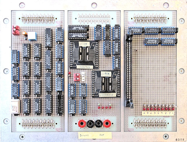
This PAL-based DRAM test board designed by Ahmad Ghaemmaghami for Fujitsu was developed to test 256Kbit and 1Mbit DRAMs. It could perform “all-ones,” “all-zeroes,” checkerboard, and inverse-checkerboard memory tests.
Ghaemmaghami’s board is an excellent example of logic design in the mid 1980s. It mixes many inexpensive TTL MSI and SSI chips with one or a few PALs, used strategically where a TTL design just won’t work for one reason or another. Note that there’s no microprocessor or microcontroller on this board. Today, 35 years later, you could likely replace all of the chips on the board with one inexpensive microcontroller.
MMI’s PALs, which were based on a number of IC fabrication technologies and testing methods going all the way back to Harris Semiconductor’s field-programmable diode matrices introduced in the 1960s, opened the programmable-logic flood gates for system designers. But these devices weren’t the final evolutionary step for field-programmable logic. Not even close. The next two rungs on the evolutionary ladder, CPLDs (complex programmable logic devices) and FPGAs, would appear shortly.
References:
Oral History of John Birkner, Computer History Museum, March 29, 2016.


Hi Steve — I agree with Max, in appreciating your deep dive into the origins of programmable logic. Thanks for the memories!
It was fascinating to hear your experience designing engineering workstations at Cadnetix, with portions of the designs not fully defined before sending to the PCB shop, and using PALs in strategic locations when the design was uncertain. Also, using PALs to decode addresses setting page sizes in memory management was common, as well as row and column address strobe (RAS and CAS) signals needed to operate early DRAMs. — Looking forward to the columns to come.