


Part 1 of this article series discussed the earliest programmable ICs that could be used to implement logic circuits. Not quite programmable logic, Harris Semiconductor’s programmable diode arrays and PROMs laid the groundwork for PLDs (programmable logic devices) to come.
This is where we return to Napoleone Cavlan, Ronald Cline, and the story of how Signetics developed the first commercially successful FPLA (field programmable logic array). Cline and Cavlan both had memory IC design experience and both joined Signetics at just the right time to participate in the next evolutionary step for programmable logic. Cavlan was in marketing and Cline was in design engineering.
Engineers were already familiar with state-machine design using programmable logic arrays (PLAs). For example, when I joined the R&D lab at HP’s Calculator Products Division in 1975, every design engineer in the lab had a copy of Chris Clare’s seminal book on the topic, Designing Logic Systems Using State Machines. Clare was a Project Manager at HP Labs. Designs, particularly chip designs based on Clare’s methodology, relied on mask programmable logic arrays (MPLAs), discussed extensively in Chapter V of Clare’s book.
In 1973, National Semiconductor introduced the DM7575 MPLA with 14 inputs and 8 outputs. National’s MPLA didn’t meet with a lot of commercial success because it was a slow device (it had a 90 nsec propagation delay) and because it needed to pass through an IC fab to add the final metal layer for characterization, which was a relatively slow and expensive process.
Integrated, on-chip MPLAs work great when you’re designing custom ICs, because you know there will be a set of custom masks involved. However, when you are designing boards, the need to design and fabricate a mask-programmed part throws a real kink into the project schedule. Systems designers sorely needed a field-programmable logic array (FPLA).
Although not commercially successful, National’s DM7575 MPLA was significant because it served as the basis for the field programmable logic array produced by Signetics in 1975, the 82S100. As Cavlan explained in his oral history:
“…in 1975, the National MPLA device was available and did not enjoy big popularity because of the fact that it was mask-programmed. Often, logic design is not a very structured process. Actually, most of the time it isn’t, if you’re talking about random logic. That’s why the name comes to mind – random logic. The inevitable changes that you would incur would not be suitable for using an MPLA, a mask-programmed device. So, the only use you could have for this part was in more structured logic like look-up tables where you knew more or less in advance what the organization was going to be and the function. But despite all of that, the MPLA was not successful.”
Cline continues this discussion later in the oral history:
“The big iron companies at the time knew what PLAs were. They used mask programmable PLAs as microcode or micro instruction generators inside their CPUs, but, again, because of what I was just telling you earlier, there was just never any consideration of the possibility. Again, after the 4K [PROM] worked, it was at about this time that Napoleone came on. As I recall, I didn’t know anything at the time. Nobody had told me.
“They didn’t want to defocus me about this other idea that was floating around, but I found on my desk a request from an engineer from Honeywell, one of the big iron companies at the time, ‘Could we make a fusable or a fused link PLA?’ That was the first time I’d ever seen the concept, but, again, it was something that… I think the technology capability, the circuit capability, the applications and knowledge, plus a built-in recognition of customer desire I think just sort of came around at all the same time.”
Cavlan then explains how the FPGA concept gelled:
“The idea was that this was a device that seemed to have a lot of general market appeal because of the success of the mask programmed devices and the desirability by people to modify logic in their design environment. So to translate that intent into the architecture was basically saying, ‘Okay, well there is a mask-programmed version available. Let’s make a field-programmable version, and make one that can be targeted to a broad range of applications that are not just bit oriented, also byte oriented.’
“And in that respect, I took it upon myself to take a look in these two areas, and I was convinced that in architecting a device that has a set of programmable AND gates and programmable OR gates but with an I/O combination which was basically byte organized (in our particular case it was 16 inputs and 8 outputs) with an enable for the output gating, it would be useful not only for generating bit logic slices out of the device…”
Using these concepts, Cline designed the first commercially successful FPLA, the Signetics 82S100. It could replace a handful of TTL chips, but it had a 50 nsec propagation delay through the part.
Cavlan details the situation in his oral history:
“The architecture of our first FPLA (82S100, PLS100) was basically an AND-OR/NOR structure because there was a polarity inversion on the outputs, I mean internally, so you could do AND-OR or AND-NOR functions. But it had a very large input width so that you could take 16 variables at the same time and put them into any one gate. Not only that but you could take a number of AND gates and distribute them at will among the outputs and also you could share them.
“So when you looked at the logic function done with TTL, usually by manipulating all those inputs, even for a single slice, you ended up with several levels of TTL packages. When you looked at that chain, the delay was sometimes much greater than just one FPLA. Sometimes the delay was smaller. It was a faster chain with TTL. In those cases, the FPLA was not the best solution, but if speed was not critical you still had the advantage of putting all those TTL chips in one package into the FPLA, one single package, and that was very useful.”
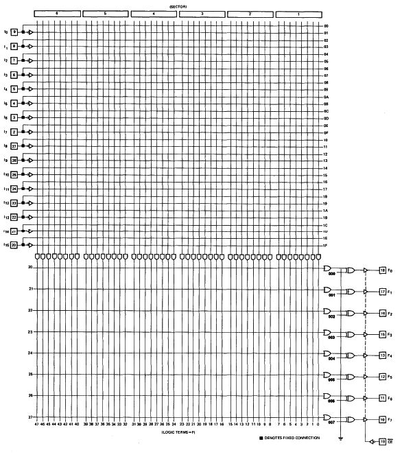
A schematic of the Signetics 82S100 appears below. There’s a fuse (not shown on the schematic) at every intersection of the horizontal rows and vertical columns.
The Signetics 82S100 sold reasonably well and was even designed into Commodore’s personal computers, including the Commodore 64. (The programmed 82S100 FPLAs in Commodore 64 computers now seem to be failing after nearly four decades in the field. The problem is sufficiently widespread to have given rise to several replacement designs built on a daughterboard using one 27C512 EPROM, a pair of PALs, or one Microchip/Atmel PLD.)
However, the Signetics 82S100 wasn’t the first FPLA. Intersil introduced the functionally similar IM5200 FPLA a month or two before Signetics introduced the 82S100. Although the two FPLAs had the same number of product terms (48), the 82S100 was about twice as fast as the IM5200, and had two additional input pins. Intersil’s FPLA was more or less obsoleted instantly. I am sure Intersil was less than thrilled about this turn of events.
The 82S100 FPLA was successful enough to encourage Signetics to expand the family with many more PLDs based on the same technology. However, the flexibility of fully programmable AND and OR arrays provided by the 82S100’s design came at a cost, literally. The die was large, which made the device relatively expensive and created an opportunity for a slightly less capable, less expensive alternative. That alternative was the PAL (programmable array logic) family from Monolithic Memories Inc (MMI). It would appear shortly, but not quite yet.
Preparing for PALs
John Birkner grew up living in a gold mine near Yosemite National Park in California. His father had caught the gold bug when Birkner was six years old and moved the family up from southern California to mine for gold. John got hooked on electronics early and became an engineer.
Eventually, Birkner started designing a line of minicomputers, called Naked Minicomputers or “Naked Minis,” for Computer Automation in Irvine, California. That’s when he started using TTL chips extensively, and that’s when he started to learn about their limitations. He also became familiar with MMI at this time because he incorporated MMI’s small bipolar PROMs in his CPU designs. These PROMs were a favorite for logic designers during this period because they were fast and they were field-programmable, which permitted fast design changes.
Signetics was also trying to get into Birkner’s minicomputer designs with its 82S100 FPLA. The Signetics FPLA should have been a perfect fit for Birkner’s minicomputer designs. It wasn’t, for several fundamental engineering reasons. As Birkner explains in an oral history:
“… I just couldn’t justify the cost, the size of those big packages, and the propagation delay was not fast enough. Nope, didn’t do it. But it kind of gelled, ‘Oh, maybe I should go up there and tell them what they need!'”
Birkner would soon get the chance to “tell them what they need.” In fact, he’d play a major role and would end up driving the next evolutionary step in the development of field-programmable logic, as will be discussed in Part 3 of this article series, next week.
References:
Signetics FPLF Oral History Panel, Computer History Museum, September 15, 2009.
Oral History of John Birkner, Computer History Museum, March 29, 2016.
Advanced Micro Devices (AMD) 22V10 Programmable Array Logic (PAL) Development Team Oral History Panel, Computer History Museum, July 19, 2012.
Stanley P. Frankel, “The Logical Design of a Simple General Purpose Computer,” in IRE Transactions on Electronic Computers, vol. EC-6, no. 1, pp. 5-14, March 1957, doi: 10.1109/TEC.1957.5221555.
C. P. Clare, Designing Logic Systems Using State Machines, McGraw-Hill Inc, 1973.


Hi Steve, interesting how Stanley Frankel’s thermonuclear simulation program on one million punched Hollerith cards ties in with National Semiconductor, Dale Mrazik’s DM7575 MPLA product definition for the IBM punched card EBCDIC to ASCII conversion requiring 96 product terms in one package. Cavlan’s FPLA 82S100 count was just half that, 48 product terms, no doubt to save die size, while increasing inputs from 14 to 16.
Thanks for the memories of my growing up living in a gold mine near Yosemite National Park in California. My fondest memory of those days was using tweezers to pick out the gold nuggets from the black sand concentrated on the end of the shake table.