


I started designing engineering workstations in 1981 for Cadnetix in Boulder, Colorado. The top computer-aided engineering (CAE) vendors of the day – Daisy Systems, Mentor Graphics, and Valid Logic (I called them the DMV) – were all founded in 1981, like Cadnetix, and each developed their own proprietary CAE software suite. The five proprietary Cadnetix workstations that I helped to design, introduced from 1982 to 1985, were all based on versions of Motorola Semiconductor’s 68000 microprocessor family (the 68000, 68010, and 68020) running a proprietary, stripped-down version of Unix (which I privately called Eunuch as an inside joke).
Daisy’s CAE software, used for logic design, ran on a proprietary Daisy version of Unix called Daisy-DNIX, on a proprietary engineering workstation called the Daisy Logician, followed by the Mega Logician. Mentor’s CAE software, used for IC layout and pcb design, ran on an early Apollo DN100 workstation under the Apollo Aegis and later the Apollo/Domain operating systems. Valid Logic Systems developed schematic capture software under a proprietary version of the Unix operating system on a proprietary workstation called the Scaldsystem. (Valid was originally named SCALD Corp, founded by the original creators of SCALD (“Structured Computer-Aided Logic Design”), a set of tools developed to support the design of the S-1 supercomputer at Lawrence Livermore National Laboratories.) Valid’s other tools for logic simulation, static timing analysis, and packaging ran on a Digital Equipment Corporation (DEC) VAX.
As you can see, there was a lot of workstation design taking place by 1981. Sun Microsystems, destined to become the 800-pound workstation gorilla, was founded in 1982. All of this workstation design, plus a robust amount of minicomputer design for DEC’s VAX and its competitors, created a perfect market for the many early forms of programmable logic. You needed fast, compact ways of developing logic for the usual stuff – address decoders, state machines, and the like – and for the more exotic memory-management hardware required by Unix systems. Eventually, the microprocessor vendors would get with it and design this memory-management hardware into their microprocessors, but, in the early 1980s, you had to roll your own.
During this period, the two main ways of designing logic was to use TTL chips or, if you had sufficient volume to justify it, design a custom logic chip. (Today, we call these custom chips ASICs, but the term had not been invented back then.) Handfuls of TTL chips took a lot of board space, which was costly in terms of pcb real estate and power consumption, and custom chips were much harder to design, costly in terms of NRE, and inserted months into your design cycle.
There was a growing need for field-programmable logic devices so that engineers could develop logic designs, build them, test them, and revise them quickly. Semiconductor vendors recognized a market opportunity and stepped up to the challenge. First came field-programmable logic arrays (FPLAs), followed by PALs, GALs, and CPLDs. FPGAs finally appeared at the top of the programmable logic food chain in 1985.
The most famous popular description of how design engineers used programmable logic back in the late 1970s and early 1980s is probably Tracy Kidder’s best-selling book The Soul of a New Machine, published in 1981. In 1982, this book won the National Book Award for Nonfiction and a Pulitzer Prize for General Non-Fiction. The book became one of MMI’s (Monolithic Memories) best sales tools.
Kidder’s book described the development of the Eclipse MV/8000 minicomputer, a DEC VAX competitor, which Data General launched in the 1980s. The logic design for this minicomputer was largely based on MMI’s PAL (programmable array logic) devices, which play a prominent role in the book. Honestly, I have no idea how a book about PALs and systems engineering can become a national best-seller. If I did, I’d be writing prize-winning best-sellers myself – but talk about PALs is getting ahead of this story. This story begins with PROMs, and maybe just a bit earlier.
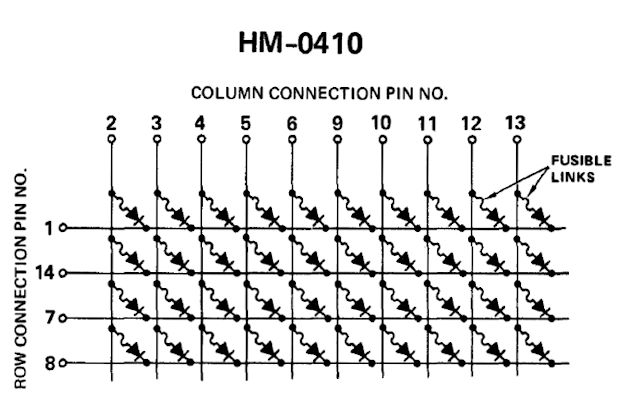
Field programmability has been an important aspect of IC design almost from the beginning of IC development. The very first programmable ICs I know about are the Harris Semiconductor HM-01xx Commercial Diode Matrices. These 14-pin DIP parts incorporated arrays of 40 or 48 silicon diodes, each nestled in a dielectrically isolated moat on one piece of silicon, and all connected by aluminum interconnect and fusible links. It took 750 mA to blow one of these fusible links. Here’s a schematic of one of those diode arrays:
Harris started marketing these diode arrays in the mid 1960s. Here’s what Napoleone Cavlan said about these arrays in a Computer History Museum oral history involving a discussion with Cavlan and Ronald Cline, who both worked at Signetics during the development of the first field-programmable logic array (FPLA), the Signetics 82S100:
“There was another element that had some modest success, which I used in 1967. These were diode matrices coupled with fusible nichrome [I believe] links manufactured by Harris. They had about 50 diodes per package,arranged in rows and columns. I used them to design a magnetic core memory simulator for a ROM as a backup for the memory on the Poseidon guidance missile. I also designed a programmer that would program these chips.”
I’ll discuss Cavlan’s and Cline’s oral history about the development of the Signetics 82S100 FPLA in Part 2 of this article series, but that’s getting a bit ahead of the story. Cavlan’s statement about the Harris diode arrays shows that integrated fusible links, a critical on-chip element needed to create early programmable logic chips, existed by the 1960s.
After reading about these Harris diode arrays in Cavlan’s oral history, I looked up the corresponding data sheet. When I first saw these diode arrays in the data sheet, I wondered what application they might be used for. Suddenly, I felt a connection snap into place. That connection transported me to a story I wrote a decade ago. It’s the story of Stanley Frankel, an early computer pioneer who was almost lost in the mists of time when I started my research. It took me three years of digging to unearth enough information about Frankel to tell his story.
Frankel fell in love with machine calculation while working for Robert Oppenheimer on the Manhattan project in Los Alamos, New Mexico during World War II. He’d been one of Oppenheimer’s grad students, and Oppenheimer took him to Los Alamos to help develop the atomic bomb. Frankel was an expert on simulation of physical processes using machine computation.
At first, he ran atomic bomb simulations on electromechanical Marchant and Friedan calculators. Frankel developed methods for farming out pieces of a large physics computation to “computers,” which in those days were women operating one of these calculators. Frankel didn’t know it, but he was developing the prototypes for solving big problems using computer algorithms. Later, Frankel moved these algorithms to new IBM tabulating card readers that Los Alamos acquired to help with the computations.
Ultimately, Frankel connected with ENIAC, the world’s first all-electronic, programmable digital computer. One of Frankel’s last tasks on the Manhattan project, just as the war was ending, was to run an oversimplified, one-dimensional simulation of a deuterium-tritium fusion reaction to verify Edward Teller’s theories about the reaction sequence inside of a hypothetical hydrogen bomb detonation. Frankel’s simulation was the first real program to be run on ENIAC. Prior programs had been just test suites created by the computer’s developers to wring out bugs in the machine.
Frankel’s thermonuclear simulation program required one million punched Hollerith cards, shipped in a train boxcar from New Mexico to ENIAC’s home at the Moore School in Pennsylvania. These punched cards contained only data. ENIAC was not a stored-program computer. You programmed it physically, a little like an FPGA, using wires to interconnect various function units to create the desired sequence of operations. Results of this particular ENIAC computation are still classified, but we do know that Los Alamos pursued development of Teller’s hydrogen bomb after Frankel returned with his results.
By 1950, Frankel – the man who successfully developed the first simulation algorithms for creating both nuclear and thermonuclear weapons for the US Defense Department – had lost his security clearance, thanks to Joe McCarthy, HUAC, and the Red Scare. Why? What crime or breach of trust had Frankel committed? Frankel’s father, not Frankel, had been a communist in the 1930s, and that’s all it took to disqualify Frankel from further work on secret defense projects.
In need of non-classified work, Frankel started a consulting practice with a colleague, Eldred Nelson, and later joined a newly formed digital computing group within CalTech’s Engineering Division in Pasadena, California. It was the only way he could continue to work with computers at the time. All computers were essentially mainframes back then.
While at Caltech, Frankel designed a computer using only 113 vacuum tubes and a magnetic drum for memory and storage. He managed to design a computer using very few active elements because he implemented most of the digital logic, including instruction decoders, using 1450 germanium diodes. As Frankel wrote in his paper describing this design: “The logical design is realized by a logical network, composed primarily of resistors and crystal diodes.”
Frankel called his 113-tube computer the “MINAC,” sort of a “minimal ENIAC.” He designed the computer in 1954, and by 1956, MINAC became a commercial computer. Librascope licensed the MINAC design from Frankel and used it to produce the desk-sized Librascope LGP-30 computer. By some accounts, the LGP-30 was the first “personal” computer. It was not timeshared; it didn’t require special air-conditioned rooms; and it ran on power from a standard 115-volt wall current. In addition to being widely used as a general-purpose computer for data processing, the LGP-30 was also used as an embedded computer for industrial testing and process control.
The diodes used in the MINAC design came from a component reject barrel at nearby Hughes Semiconductor, which had just started manufacturing germanium diodes. Hughes encouraged Frankel to take as many as he liked from the reject pile. They didn’t meet spec, but they worked just fine in logic circuits. Ten years later, Harris Semiconductor was making 40- and 48-diode arrays with field-programmable fuses and marketing them to digital designers.
Yes, that’s right. We once used nothing but discrete diodes and resistors to implement logic gates before digital ICs appeared. It was called diode logic (DL) or diode-resistor logic (DRL). Frankel reused this idea – of using lots of cheap, off-spec diodes, to implement logic functions – when he designed a desk calculator for SCM in the mid-1960s. That calculator, the Cogito 240, was indirectly responsible for HP’s entry into the calculator market. (But that’s another story, for another time.)
When I saw the data sheet for the Harris diode arrays, and the schematics for the devices, I immediately recalled the 1450 germanium diodes that Frankel used in the MINAC’s design. These diode arrays were clearly programmable devices. They could be used to build logic circuits, but they weren’t yet programmable logic devices.
A diode array data sheet from the 1984 Harris Bipolar catalog proudly proclaims that these arrays are “CMOS compatible.” It’s not clear to me what that’s supposed to mean, but that’s IC marketing for you. Perhaps it’s a reference to the array’s 20-volt reverse breakdown voltage. In theory, you could run some early CMOS logic families at supply voltages as high as 18 volts if you didn’t mind risking the chance of “riding the lightning” by inducing SCR latchup inside of the IC from a power supply voltage spike and watching the device fry as it drew unlimited supply current. CMOS latchup was a serious problem well into the 1980s. It no longer is. (Yes, that’s another story, for another time, too.)
By 1970, Harris had announced the next evolutionary step in the history of programmable logic, the bipolar PROM. The programmable elements in these small PROMs were fusible metal links, made from nichrome instead of aluminum. Bipolar PROMs can certainly be used to create lookup tables for logic circuits. They’re fine for developing small logic circuits and state machines, but with the PROM sizes available at the time, 32×8 and 256×4 bits, they offered the logic designer very few input and output pins for creating logic from PROM lookup tables.
Perhaps the bipolar PROM’s biggest contribution to the development of programmable logic was the development of the manufacturing and test methodologies needed to ensure that the PROM’s on-chip fusible links were reliable. Harris added test rows and columns to its PROM designs to allow destructive fuse testing during wafer probing. Blowing one fuse in each row and column on every device during wafer testing went a long way towards ensuring overall device functionality.
By the middle of the 1970s, all of the bits and pieces needed to create field-programmable logic chips were in place. What remained was for someone to put these pieces together and build the devices. That’s the subject covered in Part 2 of this article series, which EEJournal will publish later this week.
References:
Signetics FPLF Oral History Panel, Computer History Museum, September 15, 2009.
Advanced Micro Devices (AMD) 22V10 Programmable Array Logic (PAL) Development Team Oral History Panel, Computer History Museum, July 19, 2012.


Hi Steve, thank you for the fascinating story about Stanley Frankel’s love of machine calculations for Robert Oppenheimer on the Manhattan project in Los Alamos. I found it amazing that Frankel’s thermonuclear simulation program required one million punched Hollerith cards, shipped in a train boxcar from New Mexico to ENIAC’s home at the Moore School in Pennsylvania!
And who could forget Tracy Kidder’s “The Soul of a New Machine”? It definitely was one of MMI’s (Monolithic Memories) best sales tools.
I remember the Data General engineers becoming so addicted to designing their own chips that they would use a PAL16R8 registered PAL to perform an inverting register function rather than a 74LS374 octal register plus two 74LS04 inverters if it allowed them to get the design on to a single PC board.
Great to hear from you, John! Hilarious that engineers loved your PALs so much that they’d use a $5 part instead of a couple of sub $1 parts to save board space.
Hi Steve — I cannot tell you how much I appreciate this deep dive into the origins of programmable logic — I’m very much looking forward to the columns to come.