


I was just chatting with the chaps and chapesses at Testonica. These little scamps offer a wide range of services, including test and measurement (T&M) and design for test (DFT) analysis, FPGA-based development, embedded software development, and electronics hardware design. The thing that really caught my attention, however, is their technology to use a board’s FPGA to self-test that board.
It turns out that half of the folks at Testonica have PhDs in electronics and test. When I heard the “test” part, I felt obliged to establish my own bona fides in this area. As I’ve mentioned before, my first position after graduating from university in the summer of 1980 was as a member of a team designing central processing units (CPUs) for mainframe computers.
We captured our designs at the gate and register level of abstraction using pencil and paper. Functional test was performed by gathering the team together, showing them your schematics, explaining how your portion of the design worked, and answering their pointed questions along the lines of “what does this bit do?” and “why did you decide to do this rather than that?” Eventually, we reached the stage where everyone agreed “It should work,” at which point this portion of the functional test was complete until we actually assembled the computer, speaking of which…
When we did get a new mainframe computer up and running, one of the burn-in tests was based on an assembly language program created by some mad scientist in our lab. The idea was that the jump instructions (“Jump Unconditional,” “Jump if Zero,” “Jump if Not Zero,” etc.) were used to “click” a small loudspeaker. By clicking it at different frequencies, different notes could be achieved (a simple resistor-capacitor smoothing circuit was used to make the tones more pleasing to the ear). The different frequencies were achieved by having different combinations of instructions inside the jump-controlled loops. The clever part was that the program’s creator had taken countless hours to make it play a sophisticated piece of classical music. As a result, while you were working on some task in the lab, you were immediately alerted to any problems when the pleasant music stopped and disagreeable screeches, squarks, and similar sounds started.
After a little more than a year, two of my managers left to form a startup company called Cirrus Designs, and they invited me to join them a few months later. My first role at Cirrus was to create tests for circuit boards using a GenRad 2225 functional tester.
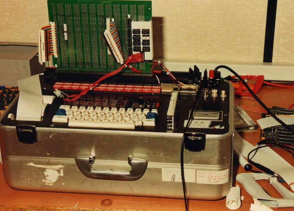
GenRad 2225 functional tester (image source: Joe Murray)
The image above shows some sort of test rig (the green board) plugged into the edge-finger connector on the tester, but this connector was usually where the circuit board provided by the customer would go. The idea is that the customer would provide us with a known-good board (oftentimes it wasn’t) and a schematic that was guaranteed to be at the same version level as the board (in my dreams).
Before we proceed, there are a few points to note. First, the boards to be tested at that time typically contained a large number of simple “jelly-bean” logic devices like the 7400-series chips from Texas Instruments (we rarely saw anything like a microprocessor). This was OK, because we all had copies of the typical component handbooks. The tricky thing came when there was a component we didn’t recognize. Remember that we didn’t have access to the internet or Google. I recall one board I was tasked with testing that had a weird component (this board was from an aircraft navigation system). It took me ages to track this component down to discover that it contained an 8×8 array of magnetic core memory.
Now, I want you to try to visualize the way this worked. I would have all the schematic sheets pinned to a corkboard-covered wall. The first statement of my program would be to pull the board’s reset signal low, so I would stick a green pin on that signal in the schematic. Then I would add additional green (logic 0) and red (logic 1) pins to indicate how the effects of the reset would ripple through the board. Next, I would de-assert the reset signal and start clocking input vectors into the board, constantly updating the state of my red and green pins. When signals eventually propagated through the registers to the board’s outputs, I would start to add tests to verify that the output pins were in the expected states. This was an iterative process, adding more input vectors and re-running the program to verify the output vectors were as expected until the board’s functionality was 100% covered.
I’ll spare you the grisly details, but the last stage was to generate 16-bit CRC values (called “signatures”) for each node on the board. The test program, including the signatures, was then delivered to the customer. Should a board fail in the field in the future, the customer would mount it on their own GenRad 2225 tester and re-run the program in test mode. The program would look to see which outputs had incorrect values and instruct the user to place a probe on one of them. The program would keep on instructing the user to move the probe, re-run the program, and compare the signatures until it found a component whose inputs were good and its outputs were bad (bad component) or a track whose signal end was good and receiver end was bad (bad track).
This whole process was called “guided probe analysis.” When I mentioned a much shorter version of all this to the guys and gals at Testonica, they looked at each other and then one of them said, “We heard about that in school.” I felt soooo old (LOL).
As an aside, as I discussed in my One More Step to Unstoppable Killer Robots blog, I’m very much looking forward to meeting the folks from Testonica at the FPGA Forum in Norway in February 2022 (see Norway & FPGA Forum, Here I Come!), but we digress…
What the folks at Testonica have done is to bring functional (and some amount of parametric) test into the 21st Century with a product they call Quick Instruments. The idea is that a large number of today’s boards feature an FPGA or an SoC FPGA. In many cases, this serves as the main processing element, accompanied by a bunch of memory, peripheral function, and communications chips.
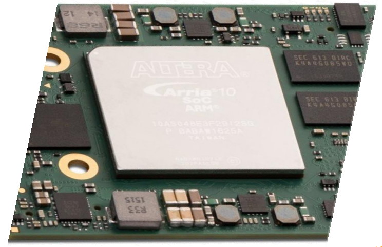
An example board featuring an SoC FPGA accompanied by memory, peripheral function, and communications chips (Image source: Testonica)
A typical scenario when prototyping a new system is that the hardware is ready before the firmware has been completed. In this case, the firmware folks are focused on finishing their functionality and are reluctant to take the time to create the code to test the board. Even worse, if problems arise when they do have code and try to run it, everyone starts pointing fingers — the software developers claim there’s a problem with the hardware, while the hardware designers remain convinced that it’s the software that’s at fault.
Enter the guys and gals at Testonica with their Quick Instruments technology. The core of Quick Instruments is a library of pre-created embedded test instruments for standard memory, peripheral, and communications devices. When provided with a description of the system, including the type/family of FPGA (Testonica supports devices from Altera (Intel), Lattice Semiconductor, and Xilinx), the types of external devices, pin maps, and register maps, Quick Instruments automatically generates and compiles the corresponding firmware test suite (observe that, in the image below, the Quick Instruments firmware test is loaded into the board’s FPGA or SoC FPGA).
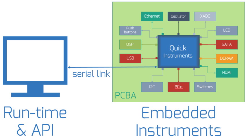
A high-level view of Quick Instruments (Image source: Testonica)
Quick Instruments tests standard devices (Memory, PHY, SFP, etc.), interfaces (LAN, PCIe, USB, etc.), and communication links (BERT, FERT, etc.). In addition to verifying the raw functionality of the board, Quick Instruments also performs some level of parametric testing that can detect manufacturing defects like an open circuit on a differential line pair, soldering cracks, opens and shorts, an incorrect PLL configuration (frequency), missing ground pins, incorrect capacitor material, crosstalk, inter-symbol interference, and metastability.
Even better, the results from the parametric tests characterized on the prototype (“golden”) board can be reused by manufacturing to test boards during production. Consider the image below:
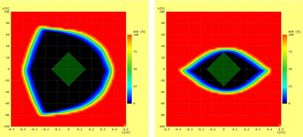
Eye diagram of good SERDES link (left) and problematic link (right)
(Image source: Testonica)
Using Quick Instruments, if the results from a good link (left) characterized on the prototype are compared to a problematic link (right) characterized on the production board, then — even though the problematic link may still function — a warning flag will be raised.
Also of interest is the fact that new test instruments are constantly being added to the Quick Instruments library as new devices and functionalities are made available to the market. In the case of Xilinx Zynq UltraScale+ RFSoC devices, for example, a new instrument is available to test the RF channels by sending a software-defined signal (e.g., sine wave) of fixed frequency to the DAC and receiving it with the ADC.
In most cases, the folks at Testonica work with test houses and contract manufacturers who deliver test solutions, but they are also happy to work directly with system design houses as required.
The classic engagement option is for the customer to send board information to Testonica (schematics, register maps, etc.), and for Testonica to return the test firmware for the board (“no muss, no fuss,” as they say). Alternatively, Testonica also provides a cloud services solution with a web interface. In this case, the customer fills in tables of things like FPGA type/family, peripheral types, register maps, etc.) and the system returns the test firmware. The folks from Testonica say that the system is so intuitive to work with that training is not usually necessary, but that it is available if required. Also, that customers may want to use the tests from Quick Instruments to augment their own functional firmware tests, in which case there is a collection of code snippets on the Quick Instruments website showing how to integrate Quick Instruments into the customer’s system.
All I can say is that test has come a long, long way since I started my career. I was going to regale you with a tale of a memory test I wrote for a mainframe computer in the early 1980s, and how pleased I was when I ran the program and it passed first time, and my chagrin when I subsequently discovered that the memory module itself had been removed from the computer and was sitting on the desk next to me, but the sands of time are racing through the hourglass and I have other fish to fry (I never saw a metaphor I didn’t like), so we shall save that tortuous tale for a future occasion. In the meantime, as always, I welcome your comments, questions, and suggestions.


