


The upshot: With a custom computing box that emulates a giant CPU/GPU pair, D2S says that they can perform full-chip ILT in a day.
Ever since the sizes of features to be printed on silicon dropped well below the wavelength of the light used to do the printing, we’ve had to monkey with the shapes on the mask. We’ve had to print not simply what we want, but some morphed form of that, replete with “assist features” that make the mask look different from what’s going to be printed. And we’ve used optical proximity correction, or OPC, to do that.
OPC is a complex stew of things to do in order to achieve a given shape in the presence of other shapes being printed at the same time. But it’s not a full, root-cause-oriented solution – and yet it works for much of a chip. That’s changing, however, as features shrink yet further.
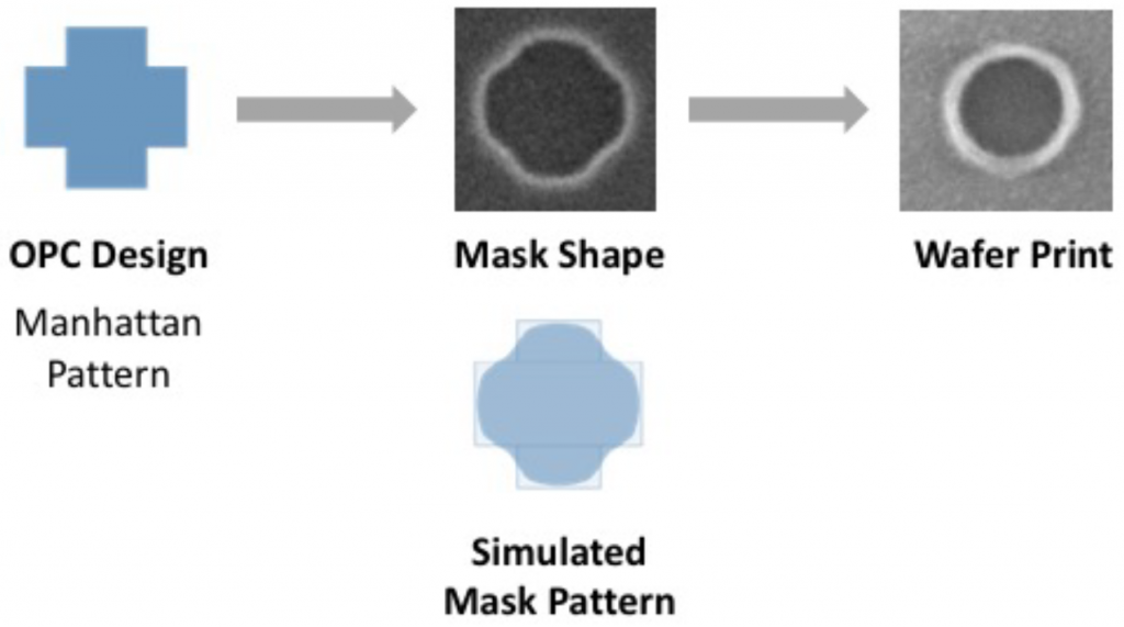
(Image courtesy D2S.)
Accurate – but Historically Slow
There is another idea that gives an exact mathematical solution to the problem. It’s called inverse lithography technology, or ILT. The idea with it is to take the final printed feature and calculate, based on first physics principles, what the mask should look like in order to achieve that feature.
And it works – with a catch: it’s been slow. As in, it takes weeks or even months to do for a full chip – an unacceptable delay when trying to get new chips to market as quickly as possible. That isn’t helped by yet another challenge begging for resolution: process windows are widest if the mask features are curvilinear. And curves have been a no-no going way back. Everything ends up being built out of rectangles: when creating the mask, the shapes have to be fractured into rectangles. Those rectangles are printed onto the mask using electron-beam (e-beam) technology, with each shot being one rectangle and with rectangles sized to minimize the number of shots. We looked at this quite some years ago.
It’s hard to make curves using rectangles. You have to use lots of tiny ones, and, even so, you’re still approximating a curve using what’s called variable-shaped beams (VSB). ILT allows true curved features to be created, but if they have to be printed as rectangles, you’re still getting something less than ideal. And the more rectangles you need, the longer it takes to create the mask.
Multi-beam for True Curved Features
The first piece of the solution is to use multi-beam e-beam writers that can create true curved features. Unlike writing rectangles, whose number and size will depend on the features being printed, multi-beam technology takes the same amount of time to write, regardless of the features.
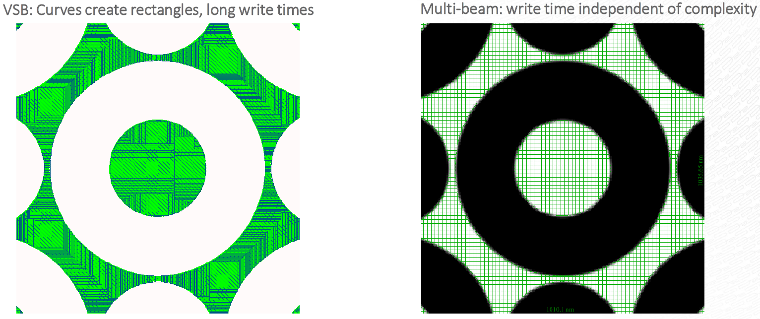
(Click to enlarge. Image courtesy D2S.)
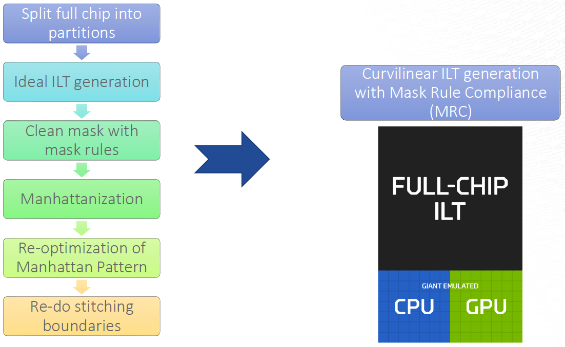
That still leaves the ILT computation time as an issue when figuring out what to print on the mask. As a result, ILT has been limited to hot spots and select areas on a chip, with the rest being covered by OPC. There are a number of issues that cause these long compute times:
- Conventional approaches using VSB still require the pattern to be “Manhattanized” – that is, converted into lines that are either north-south or east-west. Anything that doesn’t fit that description naturally has to be approximated.
- Conforming to mask rules takes yet more time.
- And the worst one: the chip must be partitioned up into tiles, each of which is calculated separately. Afterwards, the tile boundaries need to be stitched back together, and this can result in imperfections.
Faster ILT
D2S has taken a new approach to this problem, assisted in no small measure by a custom computing box that they developed. It uses many CPU/GPU pairs to emulate a single, giant CPU/GPU pair. They’ve also redone the ILT algorithms to take advantage of the massive SIMD processing that they can count on, courtesy of their new box.
(Click to enlarge. Image courtesy D2S.)
The new approach, then, is to run all of the partitions concurrently and to use real-time communication between the computing tiles to handle stitching in real time as the algorithm progresses. No more coming back to figure out the stitching after everything else is done. And mask-rule compliance is also handled on-the-fly rather than as an afterthought.
The following image illustrates what they’ve found: it shows calculated curvilinear edges created through old ILT (sequential followed by stitching) and through their new approach (concurrent). The red lines come from the old version; the blue lines are from the new version. You can see that there are stitches at edges that aren’t properly calculated the old way, but which work using the new approach.

(Click to enlarge. Image courtesy D2S.)
They’ve found that they can do a full chip up to the size of one-sixth of a reticle in a day. By reducing the full-chip turnaround, they say that they’ve made it possible to improve the yield of a given chip by rendering the entire mask – not just hot-spots – using ILT. Multiple boxes can be ganged together as well, since they’ve custom designed the inter-box communication to support using them together. You can’t speed up the turnaround by adding more boxes, but you can increase the capacity beyond the one-sixth-reticle range.
Now with Curved Features?
This capability also opens a new set of possibilities: designs that intentionally incorporate curvilinear features. Traditionally, we’ve done circuits using only Manhattan shapes – and, mostly, that’s worked – certainly for digital chips. But the Manhattan design features originated in mask-writing. The curves thing came about only when features got too small. So we used curves as a means of achieving accurate Manhattan shapes. Since we can now do curves, then why not create curved features in the original design?
Chips that incorporate curves already exist: MEMS and photonics chips, as well as specialized power or analog chips. But, in those cases, the features are large enough to be reasonably approximated by little rectangles on less-aggressive process nodes. D2S’s new ILT approach should make it possible to start with much smaller curves in the original design database, applying ILT to create modified curves on the mask that will accurately reproduce the original design curves.
Will this result in overturning the way we design chips? I’m guessing not on a large scale… Change typically makes sense only if there’s a strong benefit to it. Otherwise, momentum – or inertia – rules. Just because we can do it doesn’t mean we will do it. But as we explore new says of optimizing tiny design features, we may now have curves as an additional degree of freedom.
More info:
Sourcing credit:
Dr. Leo Pang, Chief Product Officer, D2S
Aki Fujimura, CEO, D2S


What do you think of doing full-chip ILT in the way D2S does it?