Today, we’re going to talk about AI, DSP, FPGAs, IP, and SoCs. Normally, these things don’t all go together. Certainly, FPGAs have been used to implement AI and DSP algorithms, although AI and DSP algorithms generally involve different sorts of computations. (See “A Brief History of the Single-Chip DSP, Part II .”) DSP designs have largely stayed with FPGA implementations, thanks to the bounty of multiplier/accumulators (MACs) they deliver, while AI training has migrated to GPUs. These days, AI inference has been moving to multiple hardware implementations including augmented CPUs, dedicated chips, purpose-built AI engines for SoCs, and even FPGAs. Now, Flex Logix has introduced yet another alternative: configurable hardware IP that’s specifically designed to execute AI and DSP workloads.
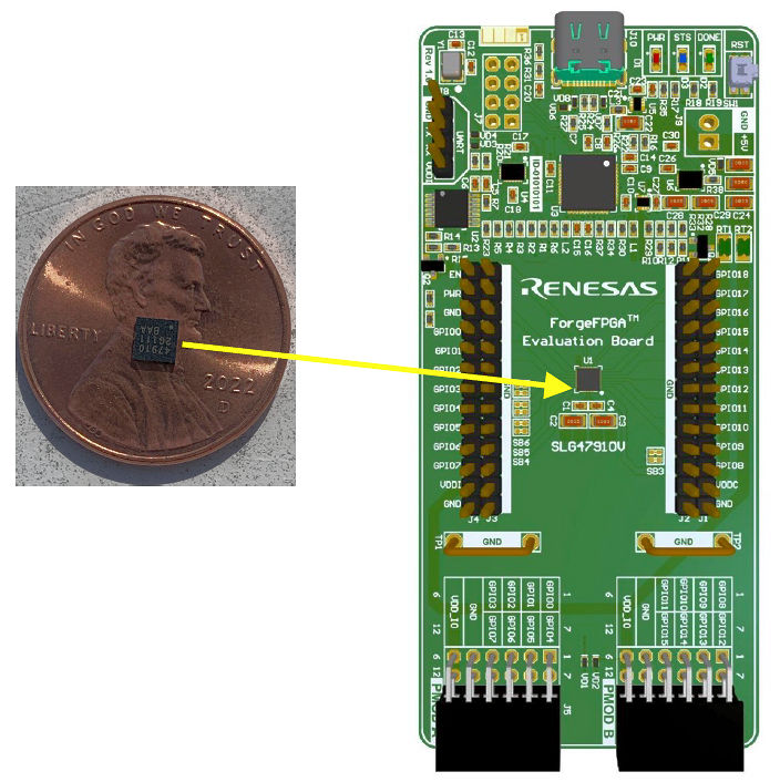
Founded in 2014, Flex Logix is no newcomer to configurable hardware IP. The company has offered EFLEX embedded FPGA (eFPGA) IP tiles and software for nearly a decade. According to Geoff Tate, Flex Logix co-founder and CEO, the company now has several defense-related customers and more than half a dozen commercial customers with 23 different chips in high-volume production that incorporate EFLEX eFPGAs. Examples of such devices range from a high-end 5G MIMO SoC from an unnamed customer that integrates a 100K-LUT (lookup table) eFPGA along with multiple transmit and receive digital front ends for the MIMO antenna interface to a new line of small and inexpensive Renesas ForgeFPGAs with 1K to 4K LUTs that can cost less than 50 cents in volume.

Figure 1: Small, inexpensive Renesas ForgeFPGAs are based on Flex Logix FPGA IP and the development tools are based on the tools supplied by Flex Logix. Image credit: Flex Logix
Renesas ForgeFPGAs trace their lineage to Silego devices, which my friend and colleague Max Maxfield has written about previously. (See “Not Much Happened, or Did It?” and “Renesas Announces Fabulous ForgeFPGA Family.”) Dialog Semiconductor bought Silego in 2017 and was in turn purchased by Renesas in 2021, which is how Renesas became an FPGA vendor. Little fish get eaten by bigger fish, which in turn get eaten by even bigger fish.
The Renesas FPGAs provide a version of the Flex Logix FPGA software directly to developers for configuring ForceFlex devices, which indicates that Flex Logix can provide usable software directly to system developers. That’s an important capability when entering the AI market, where you want to allow data scientists and programmers with no hardware development background to use your products easily.
In many ways, these new Flex Logix InferX hardware tiles trace their lineage back to the company’s eFPGA tiles. InferX IP tiles are hardened IP, supplied by Flex Logix to a customer for a specific IC manufacturing node at a specific foundry. In this way, InferX IP is just like the company’s EFLEX FPGA IP. In the case of the InferX IP, Flex Logix is initially targeting TSMC’s N5 5nm process node, but the company says that any FinFET process is a candidate for this IP.
Further, AI and DSP algorithms execute a large number of multiply/accumulate operations. FPGAs, including the Flex Logix eFPGA tiles, generally provide many, many multiplier/accumulators to execute all of those operations in real time, but these MACs are embedded in the FPGA fabric like the raisins in my grandmother’s delicious Friday-night rice pudding recipe, which were relatively few and far between. In an FPGA, hardened MACs are surrounded by the FPGA’s interconnect fabric to enable the creation of any sort of execution pipeline. However, AI and DSP algorithms don’t need that sort of flexibility—their calculation pipelines are far more regular—so the silicon overhead of an FPGA’s routing structures are superfluous and can be removed. That silicon overhead is significant and can be as much as 80% of the silicon in the area in and around the MACs according to Tate.
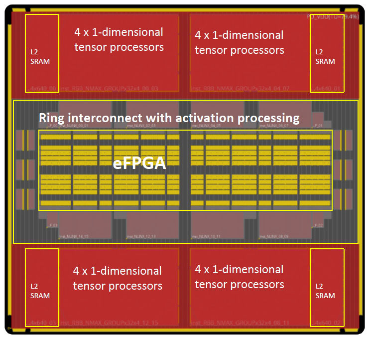
Instead, Flex Logix took its MAC design, enhanced it for AI and DSP operations, and created a hardwired tensor unit that interconnects a large number of MACs with a hardened interconnect, just the way an SoC would be designed. The resulting InferX hardware IP tile combines four of these tensor units with individual L2 SRAM caches and a smallish eFPGA that’s used to configure and interconnect the tensor units, as shown in Figure 2 below.

Figure 2: The Flex Logix InferX hardware IP tile combines four of these tensor units with a small eFPGA used to configure and interconnect the tensor units. Image Credit: Flex Logix
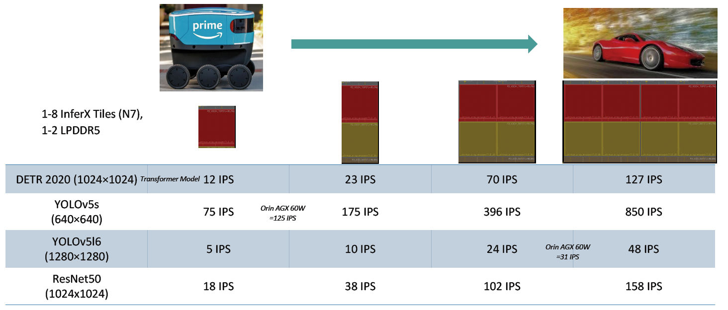
According to Flex Logix, the computational capabilities of these InferX tiles scale more or less linearly, so that the SoC development team can incorporate one tile, four tiles, eight tiles, and possibly more to meet system processing requirements. Figure 3 below illustrates the performance capabilities of 1-, 2-, 4-, and 8-tile InferX instantiations for some commonly used AI models.

Figure 3: SoC developers can instantiate multiple InferX tiles to achieve the performance level required by their application. (Note: IPS = Inferences Per Second.) Image credit: Flex Logix
As Figure 3 shows, a single InferX tile can implement multiple AI image-recognition models with varying degrees of image resolution. A 2-tile InferX instantiation roughly doubles performance compared to a 1-tile implementation, and 4- and 8-tile instantiations further boost performance. As can be seen from Figure 3, sometimes the performance boost is linear, sometimes it’s superlinear; and sometimes it’s sublinear. The performance gained by increasing the number of InterX tiles depends on memory capacity (one or two LPDDR5 SDRAMs), I/O saturation, and other system-level bottlenecks.
The required subsystem performance varies by end application, of course. A race car traveling at 200 MPH has far more demanding image-processing performance requirements in terms of inferences per second (IPS) than does a delivery robot moving at a few miles per hour. Note that the performance specifications shown in Figure 3 are for images processed per second (IPS) rather than the TOPS (trillions of operations per second) numbers other vendors use as a proxy for actual AI performance. That’s because InferX tiles are designed and configured for dedicated, real-time tasks in embedded equipment, so they’re scaled and programmed/configured accordingly. Tate says that if the prospective customer starts asking about TOPS, then the salesperson is probably talking to the wrong prospect. According to Tate, it’s the performance for specific AI model(s) that’s important for SoCs that are candidates for InferX tiles.
The software that Flex Logix provides to InferX customers does not expose the FPGA configuration or tensor engine programming directly to developers. Instead, the developer starts with an AI model trained within a machine learning framework such as Caffe, TensorFlow, PyTorch, or mxnet. These trained AI models all employ floating-point arithmetic, which is not needed for inference, so the first step in converting the AI model for use with the InferX tile is a model quantizer, which converts the floating-point values into 8-bit integers. After that, a graph compiler and operator compiler map the model onto the InferX architecture to emit an InferX run-time configuration, which the company calls “Softlogic,” and driver software with API calls. Because the InferX hardware IP is configurable, AI models can be swapped out for new ones in microseconds, in a manner similar to the use of software overlays for microprocessors. Taken together, the company collectively calls the InferX tile and AI software “InferX AI.”
For now, AI applications may get the lion’s share of press and hype, but Flex Logix has found that the primary use for its InferX tiles at the moment is for DSP algorithms, which also need to execute a lot of MACs. So, the company has created a similar package of InferX tiles and DSP software, conveniently called “InferX DSP.” According to Tate, the primary market for InferX DSP is for the replacement of Xilinx devices, specifically Xilinx Versal FPGAs and Zynq SoCs and MPSoCs, which combine Arm CPUs with Xilinx FPGA fabric. If a company is already going to the effort and expense of designing an SoC to replace these off-the-shelf Xilinx devices, there’s a potential cost savings to be had by incorporating one or more InferX tiles into the SoC to perform the MACs.
Flex Logix provides high-level software that implements popular DSP algorithms such as FFTs, FIR filters, and complex matrix inversions. For both InferX AI and InferX DSP, the resulting IP block runs as a slave accelerator, connected over an AXI interface. Because of the nature of DSP, Flex Logix also can supply a dual-ported, streaming interface to the InferX tile. Because most DSP customers already know which algorithms their designs need, the overall SoC design cycle is currently much shorter for designs that use InferX DSP, compared to InferX AI, said Tate.


