

It’s a funny old world and no mistake. Just a few days ago as I pen these words, I was on a video chat with my chum Adam Taylor, who hangs his hat in the UK. If you are desperately bored and/or need something to do, please feel free to watch this video and let me know what you think.
Adam and I were both born and bred in Sheffield, Yorkshire, England, and we both attended Sheffield Hallam University, although Adam graduated 20 years after yours truly. I’d like to claim this time gap was due to Adam being a slow learner but, in fact, he’s 20 years younger (I prefer to think “less experienced”) than your humble narrator.
A Fellow of the Institute of Engineering and Technology (IET), Adam is the founder of Adiuvo Engineering and Training in the UK. In his spare time (wry smile), Adam is a Visiting Professor of Embedded Systems at the University of Lincoln, England.
Adam and I are working on a series of blogs under the umbrella name of “How to Get an Engineering Job and Keep It” (we’ve already posted Part 1 and we’d love to receive your feedback), but that’s not what I wanted to talk to you about.
The reason I’m waffling on about this here is that, as part of the aforementioned interview, I remarked to Adam that when I was a student in the late 1970s, I saw an advert for a single board computer (SBC) in Practical Electronics magazine. I no longer remember the name of this SBC, but I do recall its being a bare board carrying an 8-bit microprocessor with a clock speed of 1 MHz, 1 KB of ROM, 1 KB of RAM, a hexadecimal keypad, and a few 7-segment displays that were used to display the address and data.
I cannot tell you how much I yearned to call this little beauty “my precious” (I still do, in fact), but it was substantially outside my budget at that time. I also remember thinking that I doubted I would ever be able to afford a computer of my own. This causes an ironic smile to flit across my face today as I consider the myriad computer systems scattered around my home and office.
I also have to keep pinching myself when I consider the specifications of today’s systems and compare them with those early machines of yesteryear. For example, the Apollo Guidance Computer (AGC), which almost crashed-or-landed Apollo 11 on the moon before Neil Armstrong took over, boasted a 0.043 MHz clock and only 4 KB of RAM, which wouldn’t have been enough memory to hold the characters comprising this column. By comparison — currently sitting on my desk, I have a “scorching hot off the production line” Jetson Nano 2GB Developer Kit from NVIDIA.
It’s amazing to think that NVIDIA’s original Jetson, the TK1, was introduced in 2014, which is six years ago as I pen these words. This was followed by the Jetson TX1, Jetson TX2, Jetson AGX Xavier, Jetson Nano, Jetson Xavier NX, and — now — the Jetson Nano 2GB. The various Jetson platforms are widely used in diverse fields such as robotics, intelligent video analytics, machine vision, and the AIoT (see also What the FAQ are the IoT, IIoT, IoHT, and AIoT?).
The official publicity photo for the Jetson Nano 2G kit is shown below, as is the real-word kit on my desk. Can you tell which image is which?
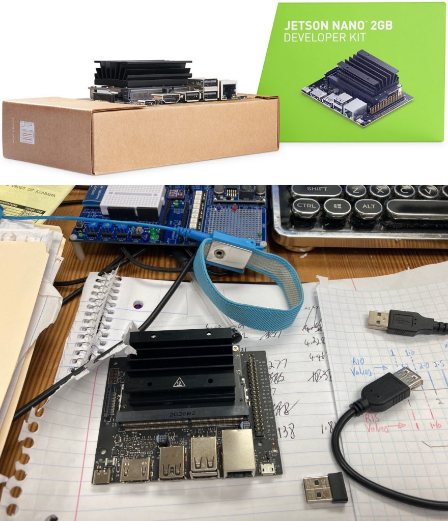
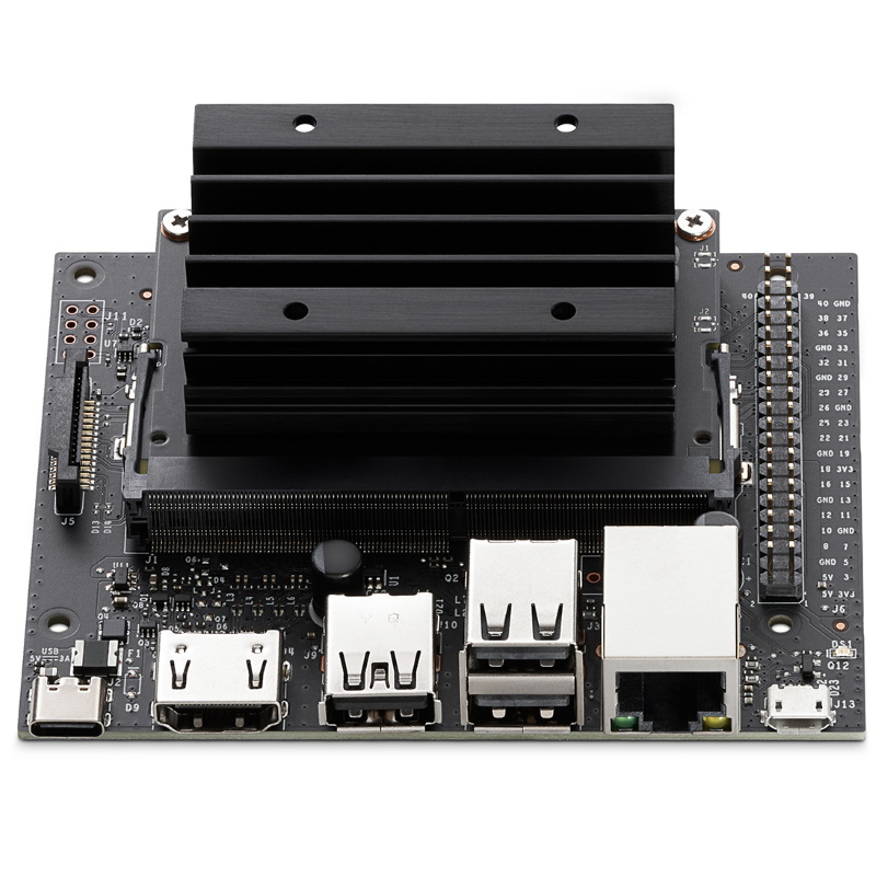
NVIDIA’s Jetson Nano 2GB Development Kit.
This bodacious beauty boasts a 128-core NVIDIA Maxwell graphics processing unit (GPU), a quad-core 64-bit ARM Cortex-A57 central processing unit (CPU), and 2 GB of 64-bit LPDDR4 25.6 GB/s memory. Additional storage is provided via a microSD card (I have a 64 GB card, but you can go much higher — for example, you can get microSD cards up to 1 TB, the thought of which which makes my eyes water).
Targeting artificial intelligence (AI) at the edge, this “entry-level” (their words, not mine) development kit costs only $59, which I think is an amazingly good deal.
The Jetson Nano 2G Development Kit has been designed from the ground up to facilitate the learning and teaching of AI. In order to support all of this, NVIDIA has announced the availability of free online training and AI-certification programs. In turn, these programs will serve to supplement the numerous open-source projects, how-tos, and videos contributed by thousands of developers. Speaking of which, the chaps and chapesses at NVIDIA tell me that there are currently 700,000 active developers in the vibrant Jetson community.
As is the case for all of the Jetson platforms, the Jetson Nano 2G is supported by the NVIDIA JetPack SDK (software development kit), which comes with NVIDIA container runtime and a full Linux software development environment. This allows developers to package their applications for Jetson with all its dependencies into a single container that is designed to work in any deployment.
The JetPack SDK includes the latest Linux Driver Package (L4T) with the Linux operating system and CUDA-X accelerated libraries and application programming interfaces (APIs) for Deep Learning, Computer Vision, Accelerated Computing, and Multimedia. It also includes samples, documentation, and developer tools for both host computer and developer kit, and it supports higher-level SDKs such as DeepStream for streaming video analytics and Isaac for robotics.
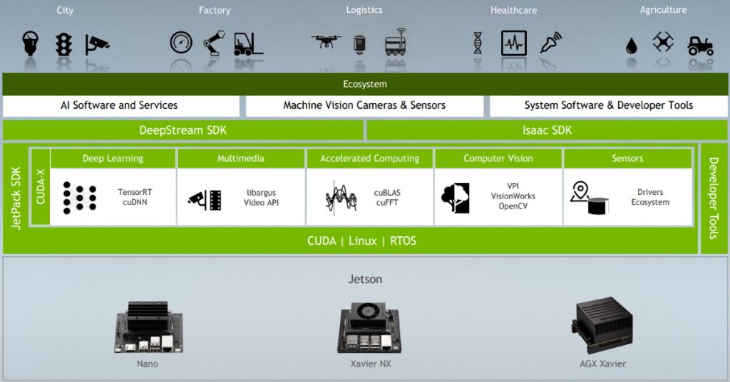
One problem with software guys and gals is that they tend to assume everyone knows what they are talking about. The diagram above, for example, shows the term CUDA, and their literature says that the Jetson SDK is “powered by the same NVIDIA CUDA-X accelerated computing stack used to create breakthrough AI products in such fields as self-driving cars, industrial IoT, healthcare, smart cities, and more.”
This is obviously exciting, but just what is CUDA when it’s at home? Thank goodness for the internet, Google, and Wikipedia, is all I can say, because a quick Google reveals the following:
CUDA (Compute Unified Device Architecture) is a parallel computing platform and application programming interface (API) model created by Nvidia. It allows software developers and software engineers to use a CUDA-enabled graphics processing unit (GPU) for general-purpose processing – an approach termed GPGPU (General-Purpose computing on Graphics Processing Units). The CUDA platform is a software layer that gives direct access to the GPU’s virtual instruction set and parallel computational elements, for the execution of compute kernels.
The CUDA platform is designed to work with programming languages such as C, C++, and Fortran. This accessibility makes it easier for specialists in parallel programming to use GPU resources, in contrast to prior APIs like Direct3D and OpenGL, which required advanced skills in graphics programming. CUDA-powered GPUs also support programming frameworks such as OpenACC and OpenCL; and HIP by compiling such code to CUDA. When CUDA was first introduced by Nvidia, the name was an acronym for Compute Unified Device Architecture, but Nvidia subsequently dropped the common use of the acronym.
I’d like to say that reading this makes me feel a lot better. What the heck, let’s go for it: “Reading this makes me feel a lot better.” Furthermore, I just ran across this handy-dandy video featuring NVIDIA’s Autonomous Machines Program Manager, Phil Lawrence, who seems to be a jolly nice person.


Different motors can be used in medical instruments. Maybe u will be interested in it! http://metonec.com/
These look great, the only problem is there are NONE available anywhere (sad face here).
Well, I did manage to find some advertised at 4X plus the listed prices, so still not really an option. Too bad, I would have loved to have spent time with the full-up JETSON NANO DEVELOPER KIT.
This is your lucky day — I have a spare one unopened here in my office — it’s yours for the asking — email me at max@clivemaxfield.com
Well, I did manage to find some advertised at 4X plus the listed prices, so still not really an option. Too bad, I would have loved to have spent time with the full-up JETSON NANO DEVELOPER KIT.