

When I worked on my first ASIC deep in the mists of time that we used to call the 1980s, we employed a traditional “waterfall” model for our design and verification flows. In this case, any activities associated with the project were broken down into linear sequential phases, where each phase depended on the deliverables from the previous one.
The term “shift left” first entered our collective consciousness in 2001 (see the original Shift left Testing article in Dr. Dobbs). It was coined in the context of software testing by a software developer called Larry Smith. The idea was that moving testing to the left on the project timeline—where time is represented as progressing from the left (past) to the right (future)—offered many advantages. Since that time, the shift left philosophy has been applied in many industries and across many engineering disciplines and tasks, including IC design and verification.
I was just chatting with Jeff Wilson, Director, DFM Product Management, Calibre Design Solutions at Siemens EDA. The focus of our conversation was a new capability called Calibre DesignEnhancer that the guys and gals at Siemens EDA introduced a couple of months ago at the Design Automation Conference (DAC) 2023. This little scamp (by which I mean Calibre DesignEnhancer, not Jeff) is the latest in Calibre’s Shift Left Solutions.
I can’t help myself, simply saying the words “shift left” makes me think of “…it’s just a jump to the left” from the Time Warp song in the Rocky Horror Picture Show (click here because we all know we want to do the time warp again), but we digress…
Since this is a complex field, let’s briefly set the scene to ensure we’re all tapdancing to the same skirl of the bagpipes. Let’s start with a high-level view of the IC development process as shown below.
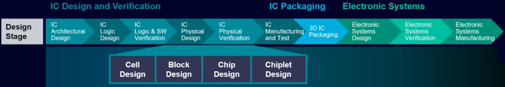
High level view of the IC design flow (Source: Siemens)
My personal playground used to be at the front-end of the process, which embraces Architectural Design, Logic Design, and Logic Verification. This is followed by the area of interest to us here in this column—Physical Design and Physical Verification—after which the design is handed over to Manufacturing and Test.
An extremely simplistic view of the physical portion of the process is that Physical Design starts when we use a place-and-route tool to place the logic cells and connect them together, and Physical Verification ends when we perform a final sign-off physical verification.
Now, this is where things start to get interesting. There are a lot of Electronic Design Automation (EDA) tools involved in this process, and there are several big players in EDA space (where no one can hear you scream). Just to increase the fun and frivolity, there are numerous smaller EDA players offering interesting point tools. The end result is that, although IC design houses may source most of their tools from one of the big EDA vendors, they may also include point tools from other vendors, both big and small.
Siemens EDA is one of the big players that can offer all the tools in the flow. Having said this, IC design houses may—of course—opt to acquire their tools from other EDA vendors. Well, not all the tools…
The one tool (almost) every IC design team on the planet uses is Siemens’ Calibre for sign-off physical verification. The reason is simple—most of the world’s semiconductor foundries use Calibre when they’re developing the design rules for their new process nodes. This means that when an IC design team uses Calibre for sign-off physical verification, they can be confident that their design will pass muster when it arrives at the semiconductor foundry.
Try to visualize the scene. When it comes to physical design and verification, your team is using place-and-route and other tools you acquired from some company or other (for the purposes of these discussions, let’s assume this company is not Siemens EDA). All the way through the physical portion of the process, your verification tools are saying “Happy dance, we’re good to go.” Finally, you run your sign-off verification using Calibre, at which point the red lights start flashing, the alarm klaxons start sounding, the blast shields start lowering over the doors and windows, and…
I’m sorry, I got a little carried away there. Suffice it to say that you are going to receive a lot of error messages, and your design isn’t going anywhere until they’ve all been sorted out. Unfortunately, a lot of this sorting out is going to involve time-consuming iterations returning to an earlier state in the process to implement changes. Even more unfortunately, some of these changes are going to introduce their own issues, which may not surface until the next time to perform (what you hope will actually be) your sign-off verification (again).
This is where Calibre DesignEnhancer comes into the picture. Before we go there, however, we should note that Calibre Design Solutions delivers a complete IC verification and DFM optimization EDA platform that speeds designs from creation to manufacturing, addressing all sign-off requirements. The Calibre Design Solutions portfolio includes Calibre Physical Verification, Calibre Circuit Verification, Calibre Reliability Verification, Calibre Design for Manufacturing (DFM), and Calibre Interfaces (which allow Calibre to integrate with all major custom design tools, place-and-route systems, and a wide range of specialty design tools).
But wait, there’s more, because—as was mentioned earlier—Calibre DesignEnhancer is the latest in a suite of Calibre Shift-Left Solutions. These include Calibre Real-Time Digital, Calibre Real-Time Custom, Calibre nmDRC Recon, and Calibre nmLVS Recon (where “Recon” is short for “Reconnaissance,” meaning “exploring,” “scouting,” and “investigating”).
With respect to the previous diagram, Cell Design refers to the physical implementation of the lowest level functional elements (cells) like primitive logic gates (AND, OR, etc.) and registers (D-Type flip-flops, etc.). Block Design refers to the physical implementation of the IP blocks (which are composed of cells), while Chip Design refers to the physical implementation of the main die (which is composed of IP blocks). More recently, we are seeing a surge in the use of chiplets (a.k.a. tiles), where each chiplet is an IC in its own right, and multiple chiplets are mounted on a common substrate like a silicon interposer (see also Are You Ready for the Chiplet Age?).
When we are designing an IC, we know there are going to be iterations between downstream and upstream processes. What we want to do is reduce the number of these iterations and shorten the time it takes to perform the ones that remain.
This is where Calibre DesignEnhancer leaps into the center of the stage with a fanfare of sarrusophones (once heard, never forgotten). This is a single product (well, a single license) with three different use models called Design Enhancer Via, Design Enhancer Power Grid Enhancement, and Design Enhancer Physical Verification Ready. The way I think of these is as point tools that can enhance the capabilities of whatever other tools the team is using—like place-and-route—by leveraging Calibre’s sign-off verification knowledge of the design rules to detect problems and fix them earlier in the physical design process.
It’s important to realize that we are talking about countless thousands of design rules. Also, that each semiconductor foundry—and each process (technology node) within that foundry—has its own rules. The easiest way to wrap one’s brain around this is to see it in action as follows. First, the physical design and verification engineers specify the foundry and process of interest. This information is used by their existing tools like place-and-route.
Bearing this in mind, let’s start with Design Enhancer Via (DE Via), which analyzes the existing layout and places additional vias, maximizing the insertion rate while still being “Calibre Correct.” Using this tool, customers may literally insert millions of additional vias. In addition to reducing the IR drop, this improves the overall robustness of the design.
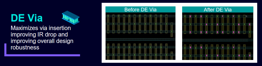
Design Enhancer Via (DE Via) (Source: Siemens)
Next, we have Design Enhancer Power Grid Enhancement (DE Pge), which is very complementary to DE Via. The power grid is traditionally a challenge—if you over-design the grid, you waste area, but if you under-design it, you’re going to stand a real risk of not being able to hit your performance requirements.
The flow here is that you create your power grid design using your regular tools. Next, you use your existing tools to perform Electromigration (EM) and Voltage (IR) drop (a.k.a. EMIR) analysis to identify any “hot spots.” Then you provide those “hot spot” windows to DE Pge, which adds “Calibre Correct” metal interconnect and vias to dramatically reduce IR drop violations and significantly improve design reliability.
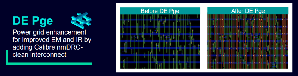
Design Enhancer Power Grid Enhancement (DE Pge) (Source: Siemens)
DE Pge has the capacity and performance to be able to handle the chip design in its entirety, so why use it only on these windowed hot spots? The answer is that doing this on the whole chip would introduce capacitance issues, so it’s preferable to employ a focused approach to solving the problem.
Last, but certainly not least, we have Design Enhancer Physical Verification Ready (DE Pvr), which is more of a traditional time-to-market play. Once you’ve run place-and-route, you are going to have open areas. These areas need to be filled with decoupling capacitors and special filler cells, all of which have their own sets of complicated rules. You could use your existing place-and-route tool to add these elements, but is it optimized for these features? Suffice it to say that DE Pvr is so optimized.
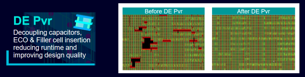
Design Enhancer Physical Verification Ready (DE Pvr) (Source: Siemens)
Will Calibre DesignEnhancer solve all your problems and eliminate iterations between downstream and upstream processes? I wish. As I said earlier: “We know there are going to be iterations between downstream and upstream processes. What we want to do is reduce the number of these iterations and shorten the time it takes to perform the ones that remain.”
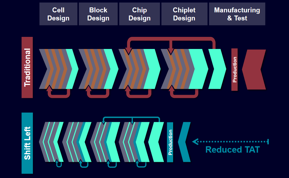
Shifting left in the physical portion of the IC design flow (Source: Siemens)
Reducing the number of iterations and shortening the time it takes to perform the ones that remain is what the shift left capabilities provided by Calibre DesignEnhancer bring to the party. In addition to reduced turnaround time (TAT), the result is to improve the quality of the design.
And the really great thing is that you can take advantage of the features offered by Calibre DesignEnhancer, even if you are using physical design and verification tools from EDA vendors other than Siemens EDA. What’s not to love?


