


Having braved several weeks hiking through the jungle, facing all the usual hazards, they find the entrance to the cavern. Only here it isn’t a cavern, but a hole barely big enough to squeeze through – after hacking away the vines and thorns that have, for centuries, protected it against intruders.
They slide in, oblivious as to what lies on the other side, driven by ancient myths, and, besting snakes and spider webs and two-headed fanged newts, they find themselves in the cavern of legend, with the priceless document resting at the base of the stalagmite, as promised. But… is the document real? Or has it been placed there as a ruse? (You’re not supposed to realize that the centuries-old vines probably make the later unlikely… that would be boring.)
“Spelunker 1: ‘My God! Just as foretold! This is it!’
Spelunker 2: ‘Wow!… But… what if it’s a fake? Do we know this is the real deal?’
Spelunker 1: ‘We need to test the material to see what it’s made of. If it’s ancient, it won’t have any modern materials.’
Spelunker 2: ‘Perfect! And how do we do that?’”
Now you need to pick from two choices. Which of these scenarios works for you?
“Spelunker 1 pulls out his phone and points it at the scroll. With no internet connection, no cloud app will work; the phone has to be completely self-sufficient. He hits a button, the app does its swirly ‘wait’ thing, and then up comes the verdict: ‘Verdict: Totally Legit.’”
Or…
“Spelunker 1: ‘I don’t know.’”
Which one would you pay money for? (OK, the dialog is awful, but hey, that’s the case with so many movies that people pay good money to see… And I blame my recent reading of a DB novel and viewing of a lame period adventure movie…)
Assuming you picked what’s behind Door number 1, then we must wonder, “How might this magic phone app work?” Well, here we enter the world of spectroscopy – plain, multi-, and hyper- and their recent developments.
Take Things One at a Time
Our first story is of the basic spectral type. Except that it isn’t specifically about a spectrometry app, but rather a mm-wave radiator sending off circularly polarized waves. Done at UC Irvine, the radiator puts out near-infrared signals in the 110-300-MHz range. They claim it to be the highest-power and –efficiency, lowest-noise radiator on record so far.
Such signals – particularly when circularly polarized – can penetrate solids, making them potentially useful for non-invasive assays of medical issues, materials, and, of course, the legitimacy of scrolls in caves.
But that’s not all. In fact, such waves can do more than peer into your deepest secrets. They’re also holding out hope that this can form the basis of the next wave – get it? – of communications technology.
Meanwhile, SiWare has announced NeoSpectra Micro, a MEMS-based spectrometer and miniaturization of their earlier NeoSpectra module. It’s intended to enable more tasks for a smartphone. At the heart of the module, they’ve taken the classic Michelson setup and implemented it on a piece of silicon.
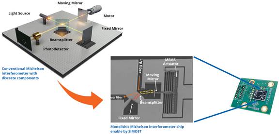
(Image courtesy SiWare Systems)
Of course, this is a conceptual drawing. The module includes a light source, which would be a broadband bulb. The sample is placed against the module; the light impinges on the sample and then enters the chip via a lens that’s also integrated into the module. Once the light enters the chip, the interferometry magic happens.
The detected range is near-infrared (NIR), between 1100 and 2500 nm; they can do yes/no and quantitative analysis. They’ve worked with partners to seed phone apps that leverage the module. As to pricing, they’re looking at high volumes at $100.
Multi-wavelength
Next comes a “multi-spectral” sensor. What qualifies a spectral sensor as “multi” rather than “hyper”? Well, certainly more than one band, but less than… some poorly defined number of bands (as described by Imec’s Andy Lambrechts). 6? 8? 10? Somewhere in that range.
And, just for a quick review here, the idea is that, rather than using a single beam of coherent, single-frequency light to test the response of a sample, multiple frequencies are analyzed at the same time. In some cases, that involves breaking a single slit’s worth of light into bands for analysis; in others… well, we’ll get to that in a minute.
Of course, you can do this with a single-frequency sensor as well, but you would need to “manually” take independent measurements for as many bands as desired. With multispectrometry, you get simultaneous measurement.
AMS has announced a 6-channel sensor targeted at the low-price sector: units run $4.00 in quantities of 1000 – intended for the phone market. Yeah, for, like, when you need to assay the provenance of a document found, oh, say, in a cave.
There are actually two sensors with different frequency ranges: the AS7262 detects visible light at 450 nm, 500 nm, 550 nm, 570 nm, 600 nm, and 650 nm; the AS7263 looks for NIL at 610-nm, 680-nm, 730-nm, 760-nm, 810-nm, and 860-nm wavelengths.
I asked how these bands were identified, and AMS’s Tom Griffiths provided some color. First of all, there’s a Gaussian wavelength response distribution about the sensor in the middle of the range; they radiate out from that in a mostly regular pattern. In addition, they’ve had some specific customer requests that explain the oddballs like 570 nm in an otherwise regular pattern.
Interestingly, he said that the near-infrared sensors, with narrower bands, tend to get used more for “yes/no” types of answers in apps like authentication and identification, while the visible-light version tends to get used more for analyzing the distribution of spectral power across the color bands.
To make this work at their price point, they credit a manufacturing technology that lays down thin inorganic interference films precisely and yet cost-effectively. They claim that these films are temperature stable and resist aging. The package is small, and power is low – critical parameters for operating in a pocket-sized device that might prove handy in a cavern.
Going Hyper
Our hyperspectral story involves Imec. We’ve looked at their hyperspectral efforts in the past, in particular with regard to a sensor they had announced. An image was either replicated on a 2D array of tiles, each of which responded to a different wavelength – “snapshot” mode – or it was scanned with a crossways slit by moving the object underneath it in “linescan” mode.
The announcement this time isn’t really about the sensor, but about a camera that combines snapshot and linescan concepts. They leveraged a portmanteau of the modes to call their camera “Snapscan,” and I was able to see it in action at their recent ITF in Antwerp.
So… how many is hyper? When you look at a plot of intensity vs. frequency as measured by Snapscan, it looks continuous – but it’s not, having 150 tightly packed bands. That would be a function of the sensor itself, but the camera adds some mechanical motion to do its work.
First, let’s look back at the linescan thing. The onus there is on the user to move the sample, which might be done using conveyor belts for inspection applications. But what if you want linescan capabilities without having to move the sample? Well, move the slit. Duh…
But doing that precisely by hand ain’t so easy. So they’ve taken care of that for you, adding a piezo element that literally moves the sensor inside the camera. When I first heard about the piezo element, I thought it was a MEMS thing. It was when I got a bigger picture of how it works that I realized that, no, this isn’t micro-on-silicon piezo; this is macro. Sort of. It’s certainly not on-chip.
Instead of taking a single image and routing it to all the sensors, they simply measure multiple lines. At any given time, one physical line is getting one test; the adjacent physical line is getting the adjacent test. Up to this point, it might sound like you’re getting only partial data, since you want both lines to get both – and all the other – tests.
This is where the motion comes in. During the one measurement we just described, that one line has only one (or a few) wavelengths sampled. But then the slit will move, and now that one line of the sample will be impinging on a different line of the sensor, giving more data. Eventually, the slit will have moved across the sample enough to ensure that the “hypercube” is fully populated.
Yeah, the hypercube. This is the name they give the not-insubstantial chunk of data that hyperspectral analysis generates. At first I pictured it as an (n+2)-dimensional set, where n was the number of bands, and the 2 represented x and y. But, with further explanation, it really is a 3D set with scalars for x and y and a vector – a value for each measured wavelength – as the third dimension.
This bundle of data does exact some overhead effort – one of the cautions regarding hyperspectral imaging more generally. If you managed to squeeze a Snapscan setup into the cavern (the camera isn’t that big, but you’ve got the stage and lighting and all), you’re going to need to bring with you the means of storing and processing.
Software is also used to improve – or equalize – the acquired images at all frequencies. If there is extra noise in certain bands, or if the sensor is known to be stronger or weaker in particular bands, then the control software can over- or under-sample to improve the quality of the data and reduce the signal-to-noise ratio.
The technologies at play here can help us to ensure that our intrepid explorers will be able to answer all critical questions at the right time – in a manner that’s credible with even the most savvy moviegoer.
More info:


What do you think about these different ways of handling spectroscopy at a micro scale?