


Intel finally succeeded in making a workable DRAM, the 1103, in 1970, and by 1972, magnetic-core memory was on its way out after a 20-year reign as the only memory of choice for mainframes and minicomputers. Compared to DRAM, core memory was slow and expensive. Access times were on the order of microseconds, and attempts to automate core-plane production met with very limited success. They remained hand-woven until the end.
One of the first computers to use DRAM as main memory was the HP 9830 “desktop calculator” developed by a renegade design team in Loveland, Colorado. The HP 9830 is arguably the world’s first real desktop computer and it was inarguably the machine that convinced me to focus my engineering career on computer system design.
As it turns out, over the last half century, every memory technology has turned out to be either slower or more expensive than DRAM. As a result, DRAM has retained the world champion title as the bulk processor memory of choice against all comers.
In the 1980s, I was convinced by a couple of Colorado memory startups that FRAM (ferroelectric RAM) would soon supplant DRAM. Didn’t happen. In the early years of the new millennium, I was expecting MRAM (magnetic RAM) to make a bid for the crown. So far, that hasn’t happened either, although you can indeed buy MRAMs from Everspin, but the parts are still small when compared with the capacities of today’s SDRAMs. The MRAM vendors are still trying.
Then came PCM (phase-change memory), but that technology has sort of dropped out of sight except for Intel’s Optane memory. Intel refuses to label Optane as PCM, but a good friend who studies these things (and the patents filed for these things) named Nathan Brookwood—an experienced industry analyst formerly with Dataquest and now research fellow at his own firm called Insight 64—assures me that Intel’s Optane is PCM.
No pretender has been able to knock DRAM off its memory throne, but If Nantero’s Bill Gervasi is right, the times they are a changin’.
Gervasi gave a Hot Chips 30 talk about Nantero’s NRAM. The “N” stands for “nanotube,” and the basic working element in the NRAM memory cell is a tiny pile of moving CNTs (carbon nanotubes) that are both attracted to and repulsed from each other by van der Waals forces. Whether these atomic-level electrostatic forces attract or repel depends on how far apart the CNTs are. If they’re closer than some critical distance, called the van der Waals contact distance, the CNTs are electrostatically attracted to each other and they stick together. If the CNTs are farther apart than the critical distance, they repel.
CNTs conduct electricity, and, when they stick together, the tangled mass of nanotubes (Gervasi called it a “stochastic array”) within an NRAM’s memory cell exhibits a relatively low resistance. When the nanotubes are spaced farther apart, cell resistance goes up because fewer CNTs are in contact with each other. There’s about an order of magnitude difference in the resistances of the NRAM memory cell’s “on” and “off” states. The result is a fast, bistable switch that can be used as a storage element, as depicted below in Figure 1, which shows a schematic representation of an NRAM memory cell.
How fast is the NRAM cell? Reads and writes are symmetric, and each take 5nsec. That’s about as fast as DRAM, but NRAM is requires no refresh cycles, so it’s actually faster than DRAM. About 15% faster according to Gervasi. (Note that the actual speed of DRAM cells hasn’t changed in many years, but increasing SDRAM block size has masked the stagnant cell speeds.)
Thanks to the van der Waals forces, NRAM cells are nonvolatile. Although a PCM cell’s non volatility has temperature sensitivity, NRAM apparently does not. Gervasi says that the NRAM cells continue to work at temperatures up to 300° C with an expected data-retention time of more than 300 years. Operate these devices at normal operating temperatures and the data-retention time climbs above 1000 years. In addition, Nantero has not observed any wearout failures in the thousands of test devices it has built. Similarly, Gervasi said that Nantero has launched NRAMs into space and the CNT memory cells show no signs of radiation susceptibility.
Forming the NRAM cells seems pretty simple, with one caveat. Deposit one set of memory-cell electrodes on a planar surface, slather on some magic sludge filled with Nantero’s special CNTs, deposit another layer of electrodes on top, and you’ve created a layer of NRAM cells. The caveat is that you need Nantero’s CNT sludge that contains only “goldilocks” CNTs, which are just the right length and just the right diameter. CNTs that are too long will short out the cell.
If you could look inside of an NRAM cell, it might look something like the drawing shown in Figure 2.
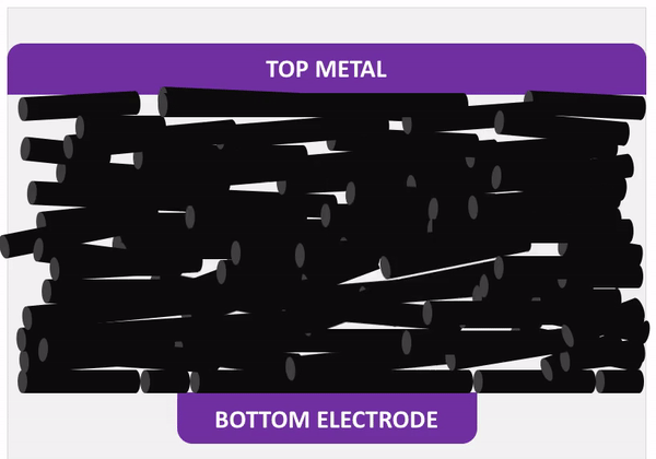
Figure 2: Illustration showing the “stochastic array” of CNTs inside of an NRAM cell. In the “conducting” state, the CNTs reach across the entire cell from top to bottom. An electrical pulse of appropriate polarity will pull many of the CNTs up, increasing the distance between the lower CNTs and raising the cell’s impedance by an order of magnitude. (Animated GIF courtesy of Paul McLellan, Cadence Design Systems)
Rinse and repeat on top of the first layer and you have doubled the NRAM’s capacity by adding a second layer of memory cells.
You can build more than DRAM replacements with NRAM, said Gervasi. You can put Nantero’s magic CNT layers on any sort of semiconductor. So, for example, you could add a non-volatile memory layer to an SRAM-based FPGA and eliminate the external Flash EEPROM.
Upon a couple of days reflection, how you might do this isn’t quite so clear to me. The NRAM layer(s) need to go on the top of the chip where the metallization is. That means the CNT layer would be interposed between the silicon die and the metallized signal and power pads. If the chip is attached to the IC package using solder bumps, as most high-pin-count devices are these days, then the CNT layer will sit between the silicon and the package. Is this layer solid or squishy? After all, you’ve got CNTs moving around in there. What’s the shear strength of a CNT layer? From Gervasi’s presentation, it wasn’t clear how or if this positioning will affect the NRAM’s or the underlying semiconductor device’s mechanical, electrical, or thermal behavior. In a subsequent email interchange, Gervasi wrote”
“The reliability team confirmed that there is no additional susceptibility to pressure than the silicon itself. The metalization through and above the array provides solid mechanical stability.”
Meanwhile, Fujitsu posted a YouTube video last April with VP and head of Fujitsu’s system memory operation Matsumiya Masato discussing his company’s plans to bring Nantero’s NRAM to market first as a memory layer for custom LSI components and then as an SDRAM replacement technology. The expected introduction date is in 2019 or possibly later. It’s important to note here that Nantero doesn’t intend to make memory devices or any chips other than test chips. Like Arm, Nantero is an IP company. Its customers make chips.
However, that doesn’t mean Nantero creates its designs without chips in mind. The company has already developed 2- and 4-layer designs for 8- and 16-Gbit NRAM devices using 28nm lithography. These designs require a chip surface of about 100mm2. The next NRAM design iteration uses 14nm lithography to build 4- and 8-layer devices with 64- and 128Gbit memory capacities. Nantero’s road map also includes a plan for 7nm, 8-layer devices with 512Gbit capacities. In fact, said Gervasi, the NRAM memory cell scales well and Nantero believes it can easily scale these NRAM cells using lithographies below 5nm.
Now this all sort of looks too good to be true, and that was Nathan Brookwood’s question to Gervasi following his Hot Chips 30 presentation. Brookwood complimented Gevasi on his talk and then succinctly asked, “What am I missing?” Gervasi replied that there was nothing to be missed here. Earlier in the talk he’d said, “These devices have been sent into space and we have data on temperature, alpha, and gamma rays. There’s nothing you can do with a CNT to get it to do something weird.” I subsequently asked Gervasi about shock and vibration. By email, he replied:
“G forces don’t overcome van der Waals attraction. Nor does vibration.”
Finally, consider this. If Fujitsu successfully brings NRAM to market, and if NRAM is as good as Gervasi says, then DRAM won’t be the only memory technology to join magnetic cores on the immense memory scrap heap of history along with mercury delay lines, Williams–Kilburn tubes, magnetostrictive wire, and bubble memory. NRAM is nonvolatile, so a successful NRAM introduction will also send Flash EEPROMs to the heap as well.
However, as discussed above, I’ve been fooled before.


So are they also EMP/ESD safe?
I do like the layer aspect that leaves them highly parallel … a few (8-32) layers of these on a really dense FPGA would make an awesome killer execution platform that is inherently high performance parallel, even with large memory demands.
I assume that somewhere, there are actually some minor QC yield issues where the tube length is violated, so that the memory requires ECC
You only said high temp’s are safe … what about on the cold side?
Will these things still function in a 3K bath tied to a quantum array?
And these babies are going to make killer Content-Addressable Memories that completely up end cache sizes, which suddenly can become GB or TB in size.
IE … data mining data base lookup size … bye bye data bases as we know them today.
using a hash as the CAM lookup key, and structuring the CAM output (physical address of the table entry) as a FIFO to allow multiple hits … done as parallel as needed for performance.
Is there even a storage hierarchy anymore?
Hmm … large rainbow tables for fast factoring and cipher breaking.
They were still getting errors after 10 Million cycles, not really sure this fits DRAM performance.
https://ieeexplore.ieee.org/document/7577997/