

Last month, Intel chucked a year’s worth of announcements into an event called “Intel Foundry Direct Connect.” Early in the event’s first two hours, Intel CEO Pat Gelsinger announced the splitting of the company into Intel Products and Intel Foundry and introduced an advisory committee for Intel Foundry consisting of four high-powered luminaries:
- Joe Kaeser, former CEO of Siemens AG
- Chi-Foon Chan, former Co-CEO of Synopsys
- Lip-Bu Tan, former CEO of Cadence Design Systems, chair of the Foundry Advisory Committee
- Tsu-Jae King Liu, Dean of College of Engineering at the University of California, Berkeley, vice chair of the Foundry Advisory Committee
Intel Foundry will make plenty of connections through these four people. Lip-Bu Tan alone has enough connections stored on his second belt phone to keep Intel Foundry busy for the next decade.
Gelsinger also pre-disclosed several new semiconductor process nodes, discussed a packaging roadmap, hailed glass substrates as the next big thing in packaging, and laid out a broad vision for an Intel Foundry ecosystem that’s already populated with most of the major EDA and IP vendors, cloud service providers, and IC design services players. To underscore the ecosystem portion of the event’s keynote presentation, Stu Pann, the head of Intel Foundry, followed Gelsinger on stage and said, “Arm is Intel Foundry’s most important business partner.” Then he brought Arm’s CEO Rene Hass on stage to join him in a quick meeting of the Mutual Admiration Society. Intel’s Processor Mafia must have had a fainting spell at that point. All this hoopla was used to underscore Gelsinger’s goal of making Intel Foundry the #2 semiconductor foundry in the world. (Uh, number two? I guess Galsinger was afraid he’d be viewed as overly aggressive or delusional if he shot for #1, at least publicly.)
That’s a lot to unpack, so let’s get to it.
Intel Foundry
Like Solomon’s biblical (almost) splitting of the baby, Gelsinger split his corporate baby into Intel Products and Intel Foundry. He’s done this to more clearly separate Intel’s foundry aspirations from the standard products that Intel has produced since the company was founded in 1968. Gelsinger said that Intel Products and Intel Foundry will be independent groups under the Intel corporate banner. This split is required if potential foundry customers are to be convinced that Intel Foundry will protect their intellectual property in the same way that other semiconductor foundries do.
Throughout his presentation, Gelsinger stressed that Intel Foundry is a system foundry, not merely a semiconductor foundry. You may feel confused at the differentiation, as I was, but upon reflection, I think it’s a little more than mere marketing. Semiconductor customers have pushed vendors to move towards systems on chips for years. Integration of systems into one package lowers overall system cost, boosts system performance, and lowers system power consumption. Gelsinger’s proposition is that Intel’s monolithic, 2.5D, and 3D packaging technologies and access to chips and chiplets (or tiles in Intel-speak) from a spectrum of process nodes and technologies allow the company to pack bigger, more complex systems into one package.
Process Nodes
Intel has spent the last three years storming through ever more advanced process nodes. Gelsinger’s objective was to develop five new nodes in four years, and the company has progressed through Intel 7 (formerly known as 10nm SuperFIN), Intel 4, Intel 3, Intel 20A, and 18A. (Note: the numbers are no longer tied to any physical measurement and haven’t been since before FinFETs first appeared more than a dozen years ago.)
During the event, Gelsinger said that chips built on the Intel 7 and Intel 4 process nodes were now shipping in volume. The Intel 3 process is qualified and ready for volume manufacturing. Intel 20A is the company’s first node to combine PowerVIA backside power-distribution technology and RibbonFETs (Intel’s name for gate-all-around (GAA) FETs). During the event, Gelsinger posed with five wafers representing the five process nodes.
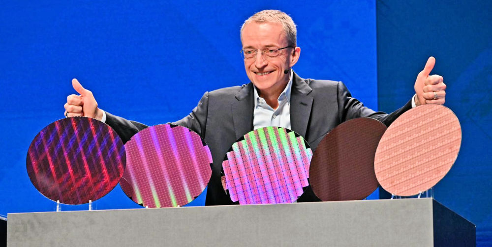
Intel CEO Pat Gelsinger poses in this “family photo” with wafers from each of the five new process nodes: Intel 7, Intel 4, Intel 3, Intel 20A, and Intel 18A. Image credit: Intel
Gelsinger also announced a new node, Intel 14A, that will be based on ASML’s high numerical aperture (High-NA) EUV lithography system. (Later during the event, Intel announced that the Intel 10A node will follow in late 2027, about a year after Intel 14A appears.) Here’s the process roadmap that Gelsinger presented at the event:
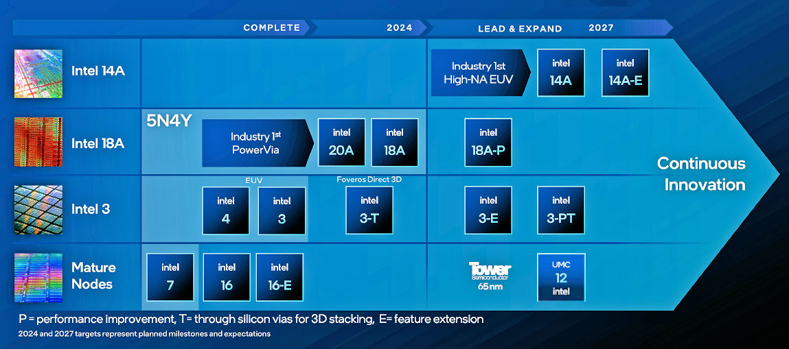
Intel presented a new process technology roadmap at the Intel Foundry Direct Connect event in February. Image credit: Intel
During the same talk, Gelsinger explained that Intel would augment many of the existing nodes with modifications that offer enhanced performance (P), through-silicon vias for 3D chip stacking (T), and feature extensions (E). These new intermediate nodes also appear in the above roadmap. The existing Intel 16nm, Intel 3, and Intel 18A process nodes will get process extensions, as will the yet-to-be-developed Intel 14A node. The roadmap also shows the 65nm planar BCD (bipolar-CMOS-DMOS) process node that Intel will be manufacturing for Tower Semiconductor, as announced last September, and the 12nm FinFET CMOS node that Intel jointly announced with UMC in January.
Semiconductor Packaging
Building silicon is one thing. Packaging the silicon so that signals reach the rest of the system with fidelity and extracting all the heat properly are also critical. Gelsinger pointed out that Intel was an early leader in introducing organic packaging to replace ceramics many years ago. The next packaging material, he said, will be glass. (Intel discussed its glass substrate developments last September.) Many organizations in addition to Intel are experimenting with glass IC substrates, because glass offers several advantages. It doesn’t bend, so it’s a stable platform for attaching die. It’s mostly made of silicon, so its thermal coefficient of expansion is close to that of silicon. It facilitates the use of photonic I/O and optics. It’s relatively inexpensive. And it dissipates heat better than organic packages.
Physics is driving a renewed emphasis on packaging, said Gelsinger. The specific physical properties to which he referred were the speed of light, which limits signal speed and reach, and the increasing thermal challenges of system design. These characteristics drive the need for physically smaller systems, with the clear implication that future ICs would incorporate multiple die – chiplets. Gelsinger also noted that Intel would be using two packaging techniques for 2.5D and 3D packaging in these advanced systems in a package: EMIB (embedded multi-die interconnect bridge) and Foveros. Both technologies are already used in shipping Intel products.
Intel Foundry Ecosystem
Beyond the glitz of bleeding-edge semiconductor nodes and package substrates made from a material that’s closely related to Swarovski crystal (glass), I consider the various ecosystem announcements at this event to be equally important for rocketing Intel Foundry to its coveted #2 position. And, when it came time to name Intel Foundry’s partners, the presentation was more than the usual logo list, which appears in the image below.
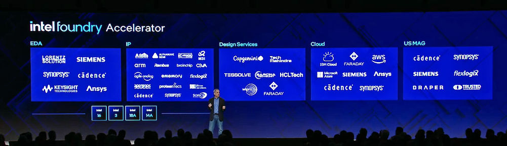
Intel Foundry GM Stu Pann unveils the logos of partnering companies in EDA, IP, Design Services, Cloud Services, and the partners participating in the specialized Military/Aerospace projects group. Image credit: Intel
One of the problems Intel has had to deal with in the past is that Intel used its own EDA tools and it expected its foundry customers to do the same. Intel Foundry’s EDA logo list now features the big three EDA companies – Cadence, Siemens, and Synopsys – as well as Keysight and relative newcomer Ansys. (Note: Synopsys recently announced that it plans to acquire Ansys.) All these EDA companies except for Ansys issued press releases, concurrent with the event, declaring their support for Intel Foundry and certification of their IC design flows for Intel 18A. By welcoming these EDA companies into its ecosystem now, Intel Foundry can assure prospective customers that they can use the IC design tools and the design flows they choose, not the ones Intel chooses. The list of cloud services partners may be somewhat surprising, until you realize that many or most IC design teams now use EDA tools in the cloud, which is essential for the work of around-the-clock and around-the-world design teams.
The Intel Foundry IP partner list is a collection of the world’s top IP vendors. In addition to Arm (mentioned above), the IP partner list includes Andes, Cadence, MSI, Rambus, and Synopsys. Of key importance: that IP list includes at least four non-x86 processor architectures including Arm and RISC-V microprocessor cores, as any significant semiconductor (or system) foundry’s partner list must. As Stu Pann explained, most of the chips TSMC manufactures incorporate Arm cores. Intel Foundry must be inclusive to compete. Intel’s maniacal x86 chauvinism has been a stumbling block for its foundry businesses in the past. No longer. Intel’s IP partners bring a ton of widely used and essential IP including multiple processor and DSP cores under Intel Foundry’s tent.
All in all, this Intel Foundry Direct Connect event was quite an extravaganza, with many announcements of some very big plans. Microsoft’s announcement that it would be using Intel 18A to build an AI chip seemed to almost get lost among the other big announcements of the day. Microsoft is Intel Foundry’s first formally announced customer for the Intel 18A process. Intel has mentioned that it has signed other customers Intel 18A, but previously declined to name any of them.
Gelsinger’s first task for Intel Foundry was to think big. Now, he needs to get his team to do big, so that they can scream – er – “We’re #2! We’re #2” by the time the year 2030 rolls around. So far, his team seems to be executing to plan. Call me crazy, but I once shared a limo with Gelsinger way back when he was Intel’s CTO and I ran the Microprocessor Forum. I find it hard to believe that he’s merely shooting for the #2 semiconductor foundry slot. Ever since that shared limo ride, I’ve known that Gelsinger is more aggressive than that. He certainly didn’t do #2 then, and I suspect he doesn’t do it now.
As a veteran CEO, Gelsinger understands the value of appropriately compensated stretch goals. So, I guess we’ll need to wait and find out where Intel Foundry ranks in six years or so. Meanwhile, don’t expect TSMC to stand still. The battle is joined, and the semiconductor industry as a whole will benefit from the competition.
For more information about Intel’s advanced semiconductor nodes, see my recent EEJournal article titled “Will 2024 Really Be Intel’s Year to Retake the Lead in Semiconductor Process Technology?”


Foundry is another word for co travt manufacturer. Not impressive that Intel “landed” a low profit, low asp job with no IP when they had the business for many generations. Microsoft used them for Intel VR11HC, VR12HC, VR13HC, and VR14HC until the icelake debacle. Now the person who was in charge of the icelake delays is in charge of Altera……so they went from $500.00 per device and their own IP to being a job shop contractor (business can easily move to TSMC or Samsung) at $39.00 per device….brilliant.
To quote Taylor Swift: “And the haters gonna hate, hate, hate, hate, hate”
Steven,
Good write up and Pat’s vision is the correct one.
When ‘ASIC’ came along, it was ‘gobbling up’ all the glue logic into one package to reduce the parts, inventory, etc saving lots of money for those utilizing ASICs. This was a first generation “system” consolidation. Even late ASICs were starting to use IP Subsystems that combined digital controller, PHY and Emb. SW drivers as fully tested blocks. An improvement to lowering risks and costs to integrate these functions.
Pat is doing version 2.0 of integration but rather than approaching from the transistor/chip side, he is coming from the system level and will need to make sure that IFS’s products, collateral and marketing are all focused on the benefits of system integration to the big customers creating systems. Pat is not searching for the customers that want ASICs; he is hunting the very large corporations that can create and sell large systems. His targets are ‘whales’ with deep pockets and large markets to serve (either products or services). This should be easy to align the sales/marketing activities within IFS.
Hunting for whales is not a particularly good strategy, in my opinion. First, that practice contributed to the demise of both IBM Microelectronics and AT&T Microelectronics as ASIC vendors. “Show me your checkbook first,” the usual whale-hunting method, is definitely off-putting to customers. Second, whales are not all that common in the electronic ecosystem. Third, “whale hunting” as a metaphor is somewhat of an insensitive choice of words in today’s more ecologically sensitive environment. Whales are endangered species and somewhat rare in the ocean, and in the electronics industry. Finally, systems implementation is a long process, so that means time to revenue tends to stretch out to infinity and beyond, as Buzz Lightyear might say.
I consider ASICs to be the second wave of IC system consolidation. Gate arrays came first, with LSI Logic and VLSI Technology. Or, if you prefer, sort of simultaneously. I’ve got an article series on the history of EDA coming up that discusses this era in more detail.
This all sounds good … if they are making paper weights or boat anchors. They are totally ignoring the fact that electronics must do more than consume power and dissipate heat. Space heaters are much less expensive.
There once was a dream of Intel developing some kind of language/tool to define what these kluges do.
Yeah, I’m talking about a skill called logic design which has apparently become a lost art. The task is to define the set of inputs that are combined to produce a useful output.
Instead we have EDA to design something that has no design tools to design the input for EDA.