

If you are anything like me, you dream of having the ability to create and automatically populate your printed circuit board (PCB) prototypes in the comfort of your own office. Well, in fact you can, because BotFactory’s SV2 combines a conductive ink printer, solder paste extruder, pick-and-place machine, and reflow bed into a single product that allows you to prototype your PCBs in a matter of minutes.
I’m starting to feel like an old fool (but where can we find one at this time of the day?). A couple of months ago, for example, I was video chatting with the chaps and chapesses at Testonica. As you may recall, if your PCB features an FPGA, these little scamps have the ability to take your schematic and register map and automatically generate a sophisticated board test suite that runs on your board’s FPGA (see Got FPGA? Got Test!).
The reason I mention this here is that, in order to establish my own bona fides in test territory, I described the guided-probe techniques we employed in the 1980s to create functional tests for our PCBs. When I mentioned this to the folks at Testonica, they exchanged a quizzical glance with each other and then one of them said, “We heard about guided-probe in school.” He didn’t actually articulate words like “antediluvian” or “antiquated,” but they were certainly implied, and I even sensed the word “prehistoric” rearing its ugly head. I felt soooo old.
More recently, I was video chatting with J.F. Brandon and George Kyriakou, who are VP Marketing & Business Development and COO at BotFactory, respectively. I don’t know why I can’t learn to keep my mouth shut. I can’t help myself. Since the topic du jour was prototyping circuit boards, I felt obliged to mention my own background in this area. Once again, these experiences date to the 1980s.
The first technique we used was that of wire wrap. Imagine a long pin protruding from the bottom of a piece of insulating board substrate material as illustrated in the image below.
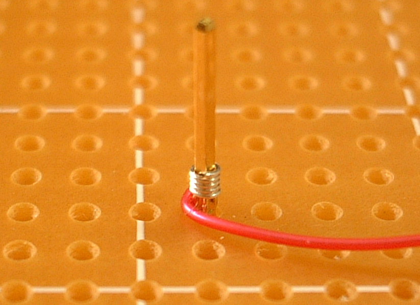
A single wire wrap connection (Image source: Wikipedia/Haragayato)
You could use a manual tool to strip the insulation off the end of the wire and wrap it around the pin. There were also electrical wire wrap tools that were similar in look and feel to one of today’s electric screwdrivers.
In addition to individual pins, you could get all the usual sizes of dual in-line (DIL) integrated circuit (IC) sockets equipped with these long wire wrap pins. Admittedly, the back of a wire wrap board could end up looking rather hairy — let’s say “interesting” — as shown below.
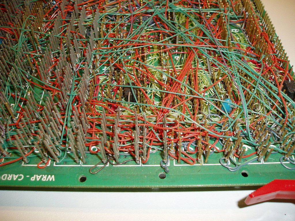
Wire wrapped Z80 computer backplane circa 1977
(Image source: Wikipedia/Wikinaut)
Although the image above may strike you as being slightly scary, I’ve worked on worse — I only wish I’d thought to take pictures of the wire wrap boards I was working on, but who knew the future would come so fast?
Where things started to get really clever was when you got to work with automated wire wrap machines. Manufactured by the Gardner Denver Company in the 1960s and 1970s, these bodacious beauties were capable of automatically routing, cutting, stripping, and wrapping wires onto electronic backplanes or circuit boards. Originally, these machines were driven by wiring instructions encoded onto punched cards or paper tapes. By the time I got to play with one in the 1980s, we used a VAX-11/750 minicomputer to drive things. We specified the X/Y locations of the IC sockets and other pins, captured a netlist along the lines of “Pin 6 of IC2 is connected to pin 8 of IC 14,” and Bob was your uncle (or aunt, depending on your family dynamic).
I remember leaving our machine running overnight. I was going to say it was located in the corner of the lab, but that would diminish its presence. In reality, it was a bit of a monster that occupied a substantial part of our workspace. All I can say is that it was truly amazing to come back in the morning to find your prototype board ready and waiting to be populated and debugged.
Another form of board prototyping technology with which I worked in the 1980s was called discrete wire technology (DWT); the resulting boards were called discrete wire boards (DWBs). Other terms we used were Multiwire and Microwire, which were registered trademarks of Advanced Interconnection Technology (AIT), Islip, New York (I’m not sure if this firm is still in business). This involved an insulating board being covered with a thin layer of adhesive, called the wiring film, which was applied using a hot roll laminating machine. A special computer-controlled wiring machine was used to ultrasonically bond extremely fine insulated wires into the wiring film. Due to the fact that these wires were insulated, they could cross over each other without making unwanted connections.
There was a lot more to this than I have the time (or energy) to cover here. The point is that, when I mentioned this to the BotFactory folks in our conversation, J.F. exclaimed, “No way! That was a thing?” And, once again, I felt soooo old, but we digress…
You may recall hearing about the BotFactory circa 2015 in the context of their first-generation PCB printer, which was called the Squink (could this moniker possibly be derived from “squirts ink”?). As you can see from this video, the Squink was impressive in its own right, and things have progressed tremendously since then.
The BotFactory’s latest and greatest offering is the SV2, which comes in three flavors according to your needs: the SV2 – Starter, the SV2 – Enhanced, and the SV2 – Professional.
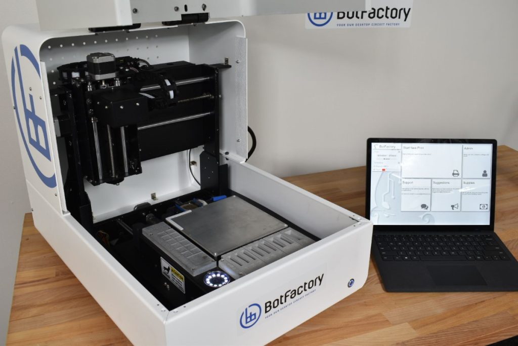
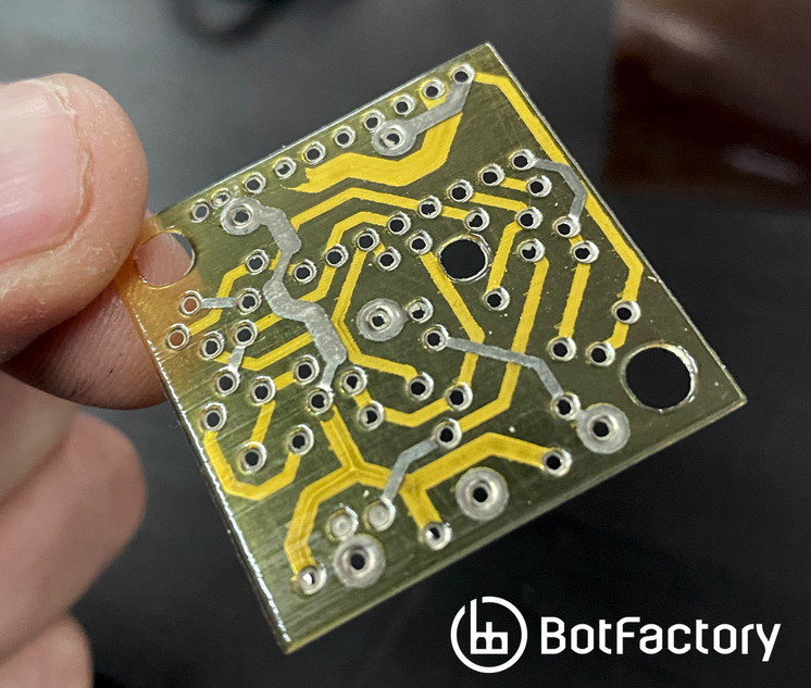
The SV2 combines a conductive ink printer, solder paste extruder, pick-and-place machine, and reflow bed into a single product that allows you to prototype your PCBs in a matter of minutes (Image source: BotFactory)
The SV2 has multiple heads to perform its varied tasks, and it automatically swaps between heads as required. First, it uses its print head to lay down layers of conductive and insulating inks onto a substrate so as to create a multi-layer circuit (multiple substrate materials can be used in addition to traditional FR4), whose track widths can be as small as 8 mil. Next, it uses its paste head to deposit conductive glue or solder paste where the component pins will be placed. The pick-and-place head is then used to automatically place the components on the extruded paste. These components may be presented on tape or via a multi-compartment tray (each “waffle tray” can hold up to 80 different component types). Finally, a curing/reflow process is employed where the heated bed cures the inks/glue and reflows the solder paste.
Although they aren’t part of the main offering, the guys and gals at BotFactory have created additional heads for certain customers, like a test/verification head that can measure the values of the various components, and a laser head that can be used to cut shorts, repair tracks, and even shape the substrate. Speaking of which…
Since I come from the era of lead through-hole (LTH) circuit board implementations, one of the things I asked about was if there was also a drill head that could be used to drill holes in the substrate. The answer is “No” (sad face). However, it turns out that some people are working on “substrate-less” boards (happy face). The idea here is that, instead of printing conducting and insulating inks onto a substrate, you can start by printing a thick layer of insulating ink directly onto the SV2’s bed, where this layer effectively becomes the substrate. This means that you can create your substrate in any shape, and you can also print it with holes in the desired locations.
You can even print a substrate-less board (Image source: BotFactory)
In fact, if you look closely at the image above, you can see that it appears they actually started by printing a thin layer of conductive ink (copper, in this case), followed by a thick layer of insulating ink, completed by another thin layer of conductive ink (silver, in this case), thereby creating a double-sided board. When you come to think about it, there’s nothing intrinsically stopping us from creating multiple conducting/insulating layer pairs on either side of the main insulating substrate layer — and this includes things like creating blind and buried vias. There’s also the potential for creating 3D electronics and 3D boards shaped to their enclosures, but I fear I may be peering too far into the future.
The BotFactory SV2 isn’t for everyone. It’s great for medium-technology prototyping (it can currently pick-and-place surface-mount devices (SMDs) down to 0603 size packages and devices with 0.4 mm pitch pins), but it cannot — at this time — handle high-technology prototyping involving components presented in 0402 and 0201 packages or medium-and-up-sized ball grid arrays (BGAs).
Having said this, while the SV2 might not satisfy the needs of people designing at the cutting edge of technology, it’s perfect for someone who is involved in academic research or for people working in labs creating electronic devices to support others in their research and development tasks, to provide just two examples. In fact, the more I ponder on this, the more I think the SV2 could be of interest to many small and medium (even large) companies who need to get their hands on their prototype boards as quickly as possible. It doesn’t take many cycles of getting prototypes in hours instead of days to cover the cost of owning your own PCB printer.
Just a few minutes ago as I pen these words, I was chatting with my chum Duane Benson, who is the marketing manager over at Screaming Circuits. These are the folks you go to if you need a few thousand short-run production boards to be populated and assembled in the shortest amount of time possible. Duane mentioned that, in the before times (prior to the current worldwide pandemic), he saw one of the earlier BotFactory offerings at a Maker Faire and, in his own words, “I was impressed.” Duane and I both agreed that we would love to have SV2s in our respective offices, which — as far as I’m concerned — is the “gold seal of approval,” as it were. How about you? Could you be tempted by an SV2 if one came your way?


While I was writing this column, I recalled my chum Joe Farr in the UK telling me that he used to make his own prototype boards (etching the copper and suchlike) in his workshop. I also recalled that, a couple of years ago, Joe told me that he’s invested in a CNC milling machine that was intended to create PCB prototypes by milling away the unwanted copper. I emailed Joe to ask him how that CNC machine was working for him, and he replied as follows:
“The milling machine ended up in the bin (well multiple parts buckets anyway). It was only cheap and I never really got it to work very well. One day I’ll try again, but right now I’m more than happy to outsource my prototype boards.”
I wonder what Joe is going to say when he reads this column 🙂
I’m a 90s kid that got my first etching kit at a RadioShack at a local mall, and then later perfected my soldering skills in the Navy. It hurts my feelings a little every time I read another article telling me to give up and send my files to a fab shop in China. I feel like hobbling to my soap box and screaming, “when i was a kid, we had to to put components THROUGH the pcb, up hill, both ways, in the snow.” I got into 3d printing a while back and have tinkered a few times with trying to make a reasonable quality pcb, to no avail. I think I felt like your friend Joe. Anyway, this was a fun read, and I’m excited that maybe the trend of home fabrication is coming back around. Cheers!
Thanks so much for your feedback — Joe also used to make his own boards — I never did, but I wish I had (I often used strip board) — I wish I had more time to work with 3D CAD software and 3D printers — my chum Steve Manley in the UK is doing awesome things regarding a robot head we’re working on. So much to do, so little time to do it all in…