

I remember seeing articles circa the mid-1980s proclaiming that optical computers were “just around the corner.” What they failed to say was that the corner in question was going to be called “2025” (if we are lucky). On the bright side, the folks at Lightelligence appear poised to push us around that corner!
I was just chatting with Spencer Powers, who is Co-Founder and President of Lightelligence, and Yichen Shen, who is the CEO for Lightelligence.
Just to make sure that we’re all tap-dancing to the same drumbeat, a brief overview of Lightelligence is as follows. Based on a bunch of research at MIT, a paper was published in Nature Photonics in 2017. The title of this little rascal was Deep Learning with Coherent Nanophotonic Circuits. In 2018, the folks involved in writing that paper spun out of MIT and formed Lightelligence.
There were a number of patents associated with the original paper, and these patents are owned by MIT, but they are exclusively licensed to Lightelligence. In 2019, the guys and gals at Lightelligence created their first photonics optical accelerator demonstration for artificial intelligence (AI). This demo, which was called COMET, involved a photonic chip containing ~100 photonic devices coupled with a Xilinx FPGA, and its first AI workload involved recognizing handwritten digits.
COMET impressed the socks off a bunch of people, including a hedge of venture capitalists (VCs), as evidenced by the fact that — just one year later in 2020 — Lightelligence had raised over $100M and had ~150 employees. As an aside, 2020 was also the year they published their Heuristic Recurrent Algorithms for Photonic Ising Machines paper in Nature Communications (I’m sure my mother would say that this paper was a real page-turner had she had the time to read it, but she’s a little busy playing Wordle at the moment).
Before we peek at the hot-off-the-press news from Lightelligence, let’s first take a moment or two to set the scene. Let’s start with the fact that, as discussed in the AI and Compute paper from OpenAI, we can split the development of AI into two distinct eras of compute usage with respect to training AI systems. The illustration below reflects AI compute requirements across multiple domains: speech, vision, language, and games.
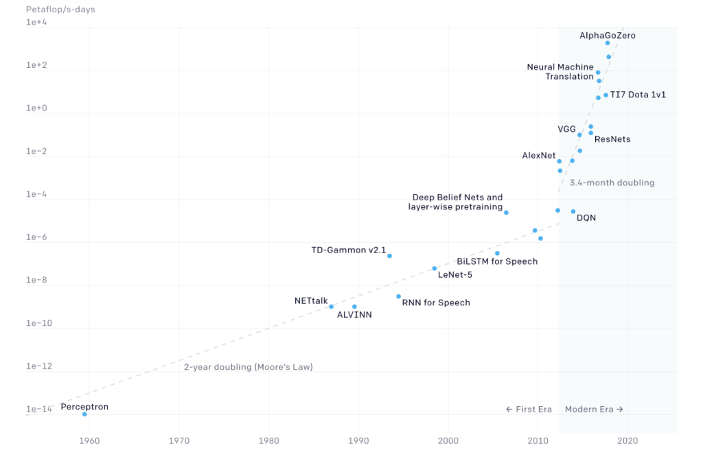
Two eras of AI compute (Image source: OpenAI).
During the first era, which took place from 1959 to 2012, there was a doubling of AI compute requirements approximately every two years, which roughly mapped onto Moore’s law. This law originally referred to the number of transistors that could be created on an integrated circuit (IC), but it’s also been used as a yardstick for compute power. By comparison, from 2012 to the present day, which we might think of as the modern era, we’ve seen a doubling in AI compute every 3.4 months!
In addition to the fact that traditional CPUs, which are largely bound to Moore’s law, are finding it difficult to keep up, electronics is starting to reach its physical limits. Yes, I know that we’ve all heard this before. My first ASIC design circa 1980 was at the 5 µm technology node. When we approached the 1 µm technology node several years later, industry pundits proclaimed, “This is the end,” which they kept on proclaiming as we sailed through the 0.8 µm, 0.35 µm, 0.18 µm, and 0.13 µm nodes, and on through the 65 nm, 45 nm, and 28 nm nodes, and… you know how it goes.
On the other hand, I fear that we really are starting to approach the physical limits of what is possible with conventional electronics. Moving from the 16 nm node to the 7 nm node, for example, gives us -60% power at the same performance, or +40% performance at the same power. By comparison, moving from the 7 nm node to the 5 nm node gives us only -30% power at the same performance or +15% performance at the same power. All of which raises the question, “Just how low can we go?”
Meanwhile, the industry is facing insatiable compute and throughput demands coupled with pleas for energy efficiency and a reduction in the total cost of ownership (TCO). The solution, according to the folks at Lightelligence, is to move to photonic computing, extending current processor offerings (CPUs, GPUs, FPGAs, and ASICs) with what they’ve dubbed “Photonic ASICs.”
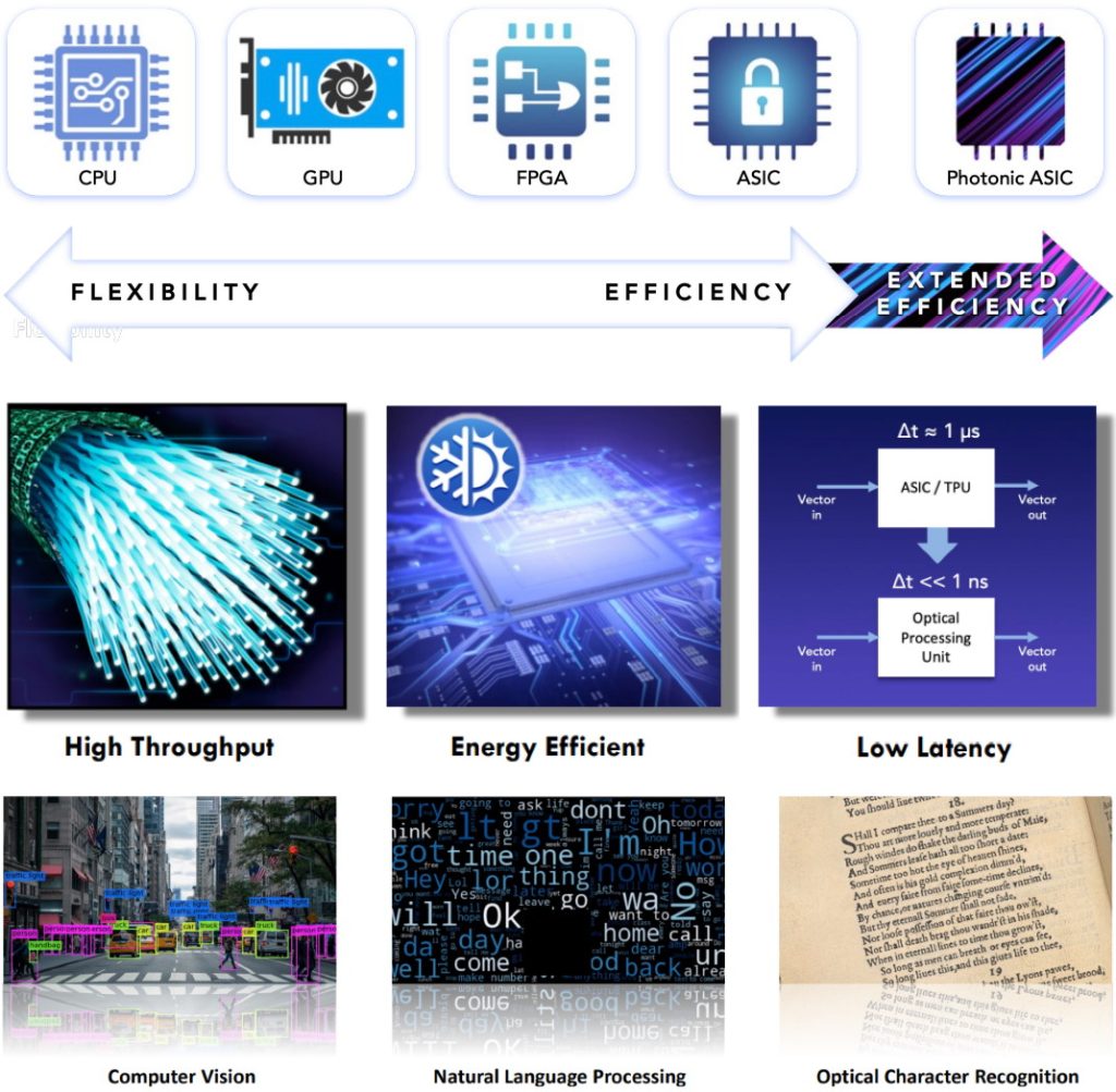
Say hello to photonics ASICs (Image source: Lightelligence).
Using photonics provides a high throughput of > 1 TB/s per channel (as compared with copper wire which tops out around 1 GB/s per channel), greater energy efficiency (there’s no ohmic heating, unlike in electronic circuits), and low latency (matrix multiplications in << 1 ns as compared to ~1 µs for an ASIC/TPU implementation).
In its current form, the photonics technology from Lightelligence has application from the cloud and data centers to on-prem servers, with markets ranging from cloud AI to finance to smart retail, and applications ranging from computer vision to natural language processing (think Alexa and Siri) to optical character recognition.
All of which brings us to a recent technical breakthrough from Lightelligence in the form of their latest fully integrated computing system — the Photonic Arithmetic Computing Engine (PACE), which is discussed in detail in this video.
In fact, PACE offers the company’s first demonstration of optical computing for use cases beyond AI and deep learning. For example, it efficiently searches for solutions to some of the hardest computational tasks — such as Ising, the graph Max-Cut, and the graph Min-Cut — which belong to a class of mathematical problems known as NP-Complete. Algorithms for NP-Complete problems have hundreds of practical applications, from bioinformatics, to scheduling, to circuit design, to discovering new materials (do you recall my column Welcome to a World of Reconfigurable Intelligent Surfaces in which I said “…I am convinced that we will soon crack the door open into the materials age…”?).
With ~12,000 photonic devices on a single chip, PACE is ~1,000,000 times faster than the prior demonstration platform, COMET (you have to admit that a 10^6 improvement in just a couple of years “ain’t bad goin’”). Although this demonstration does not show optical superiority for all applications, PACE runs this particular Ising problem algorithm hundreds of times faster than a computing unit like Nvidia’s RTX 3080, which is one of (if not the) world’s most advanced GPUs.
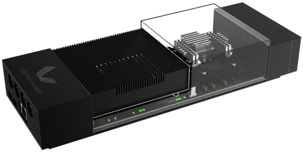
Say hello to PACE (Image source: Lightelligence).
The actual photonics ASIC at the heart of PACE is located in the middle of the module under the transparent box.
Before I get you too excited, I should note that the ~12,000 devices in the current photonic ASIC are used to implement a 64 x 64 systolic array that can perform a wide variety of linear operations like matrix addition, multiplication, and so forth (pretty much any matrix manipulation one may desire, now I come to think about it). In future products, in addition to the array itself (where the optics provide low-latency and low power), there will also be an optical network on chip (NOC) that will be used to transfer data between the array and supporting circuitry (where the optics will provide high throughput and low power), because the optical array still needs access to regular electronic memory (SRAM, GDDR, HBM, etc.), which is ideally located in the same package.
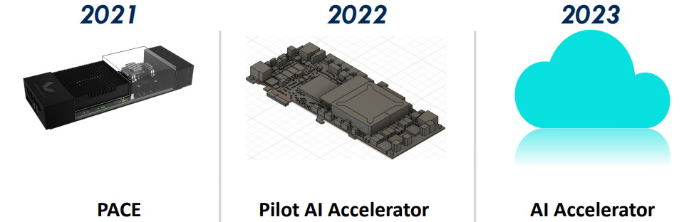
So, here’s where things stand at the moment. We currently have PACE, which is still largely a proof-of-concept. The next step is going to be the introduction of a Pilot AI Accelerator with a PCIe formfactor in 2022. This Pilot AI Accelerator will be created in conjunction with global leaders in finance and cloud computing. The folks at Lightelligence say that 2023 will see the introduction of a photonics-base cloud AI accelerator that will make me squeal in delight (actually, I think it was I who said I’d be squealing in delight, but there’s no need to quibble).
Roadmap to the optical future (Image source: Lightelligence).
Now, all of this is certainly exciting as far as it goes, and it actually goes rather far, but a photonic 64 x 64 systolic array is not quite the same as an optical computer (although, since no one has actually seen an optical computer, I might be going out on a bit of a limb here). But then I started thinking…
I attended Intel Architecture Day 2021 in which Intel announced architectural advances whose ramifications will reverberate down the years that are to come (see Will Intel’s New Architectural Advances Define the Next Decade of Computing?). Intel’s next-generation processors are going to be equipped with systolic arrays that handle all of the matrix processing demanded by AI and graphics and so forth applications. What do you think might happen if these arrays were replaced by their photonic counterparts? Also, Intel’s Embedded Multi-Die Interconnect Bridge (EMIB) technology is currently used to link multiple heterogeneous silicon dice in the same System-in-Package (SiP). Might we soon see the introduction of photonic EMIBs (P-EMIBs)?
As always, I’m left gasping in astonishment at how far we’ve come so fast, and I’m longing to see where we will be going in the future. How about you? Do you have any thoughts you’d care to share about anything you’ve read here?


not even one representation of a single circuit element ?…disappointing
Hi Gene — It’s a but tricky to show a circuit element because my understanding is that it’s all done using analog light interference (which makes my brain hurt), but I bet if you contacted them they would be delighted to tell and show you more.