

Anything you do can be done efficiently or not. Whether it’s driving (mpg?), playing sportsball (results/energy spent?), or walking the dog (who pulls whom?), you can be efficient or not. Obviously, higher efficiency is better – assuming you care (sometimes spending energy worrying about efficiency can be inefficient). So… what if you could identify an improvement for an activity you care about that, by itself, would increase your efficiency by almost 50%?
That’s what Spin Transfer Technologies (STT) is claiming with their new Precessional Spin Current (PSC) idea. Yeah, not exactly your run-of-the-mill daily activity. Before we look at those numbers, let’s back up a bit to put some context around this. We’ll review some basics here, although we did a more thorough primer on MRAM many years ago, and we have discussed STT (the company, not the “spin-torque transfer” technology) more recently (but still a couple of years ago).
Briefly, an MRAM cell consists of two magnetic layers separated by a tunneling layer. One magnetic layer, called the reference layer, is fixed in polarity. The other is “free” – meaning that its polarity can be switched. The cell then records a 1 or 0 depending on whether the two magnetic layers are parallel (i.e., both have N and S in the same direction) or anti-parallel (they’re in opposite directions). The amount of current that can tunnel through is different for each state, giving a way to read the state.
Such cells can be used in different ways. Some companies (like STT) make MRAM cells designed to be embedded in SoCs; others (like Everspin) make dedicated MRAM chips that compete with flash. And, as we’ll see, the intended application can also drive the direction of how the cell performs.
A More Efficient Cell
There’s an efficiency associated with the switching operation, and STT defines it as the thermal barrier Δ divided by the amount of current needed to induce switching. So the higher the Δ, the higher the efficiency. The higher the current required to program the state, the lower the efficiency.
The key here is the thermal barrier, effectively the barrier to switching, which keeps the state from degrading, directly impacting data retention. By adding this new PSC structure, that barrier goes up such that efficiency grows by 44%. This provides two opportunities: on the one hand, a higher barrier raises data retention – by 2-4 orders of magnitude. Alternatively, if you compensate for that higher Δ by lowering the switching current, you get the same overall efficiency as you had before, only now using less current to set the state of the cell.
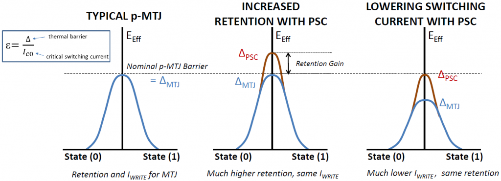
(Image courtesy STT)
If data retention is your goal, then they say that this increases the data retention from seconds to months. That gave me great pause: I’ve always thought of MRAM as a non-volatile memory, but if you can lose your state in seconds, well, that seems pretty volatile. Let’s come back to that in just a minute.
They also found that this helps temperature performance: for a constant Δ, the device will act as if it were 40 degrees cooler. They obtain the Δ value from data retention measurements, and the Δ at 100 degrees corresponds to a data retention of over one day.
Holding That Thought
Here again, that’s phenomenally short data retention as compared to flash memory at 10 years. How can MRAM be a non-volatile memory (NVM) with such short retention??
Well, it turns out that that depends on what you’re using MRAM for. There are two big gaps in the memory world: the one between DRAM and SRAM and the one between DRAM and flash (so-called storage-class memory). So it depends on which gap you want to use this for. Over time, I’ve heard about MRAM competing both based on its non-volatility – competing with flash, and, alternatively, based on its speed, lower power, and ease-of-use, suggesting it might compete with SRAM.
As it turns out, an MRAM cell can be engineered for long retention if you want to compete with flash. But if you want a super-small cell, then you can have something way cheaper than an SRAM cell that uses much less current (and no static current). And there’s no established data retention requirement for SRAM; it’s assumed to be volatile, so there’s no expectation of it sitting on the shelf and holding state.
But data retention as a spec is focused specifically on that: the chip is powered down and idle or on the shelf. There’s also the issue of holding state while powered up. DRAM, of course, can’t. That’s partly due to charge leaking away from the cell, but it’s also because the read mechanism is destructive. Each read operation is really a read-restore operation.
MRAM does not have a destructive read operation, so its data loss would be more akin to leakage. But, even though it may use way less power than an SRAM, if it remains powered up and you need the data to stick around for hours or days or whatever, then data retention on the order of seconds or days is a tad scary.
Of course, if the PSC technology takes the retention from seconds to months, then, well, that’s a big improvement. But still… yeah, there’s no SRAM retention spec, but there’s an expectation that data retention for an SRAM cell is infinite as long as the power remains on. A powered-up SRAM cell should never lose state, excepting single-event upsets (SEUs) and such. It almost seems to me that there’s no spec because it never occurred to anyone that there might be a need for one.
So, watering down that expectation could be a big deal, it would seem to me. There are a couple of ways around this. If they trade off cell size, then they can increase retention in a somewhat more expensive version. That said, if they’re competing with a 6T (or 8T) SRAM cell, then they have a lot of room to grow and still be less expensive. They raised another possibility when I talked to them about it: if the application couldn’t handle the rated retention, then a refresh facility would be easy and inexpensive to add.
Now… I don’t know about you, but I think of DRAM refresh as an extremely complex business – one that’s been abstracted away for us so that we don’t have to worry about it. It seems that adding that in to an MRAM chip would be a big deal. But STT said that it would be straightforward and simpler than DRAM refresh – especially if it needed a refresh only, say, once a day.
So, per STT, this retention issue, if it is an issue, could be made a non-issue.
A Slightly Higher Stack
Given the benefits of PSC, then, what is it? Well, we can’t say for sure. What we do know is that it adds three layers to the MRAM cell stack. What are those layers made of? That’s a secret. The image below shows where it goes in the stack.* You’ll notice that it’s what they call “modular”: it simply adds to the existing stack – whichever stack that might be, using no materials or tools other than those already used in making an MRAM. It increases the wafer cost by about $1 – pretty much in the noise.
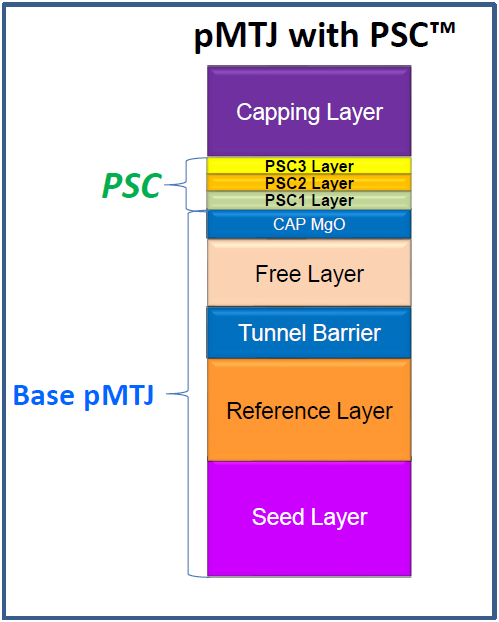
(Image courtesy STT)
Meaning, they could add this to anyone’s stack and it would help. They also say that they could likely get even better results with a redesigned stack (that is, one that isn’t modular). But modularity has benefits – including possible licensing from foundries and memory IDMs that already make MRAMs.
In fact, such discussions are underway, adding to the list of IP they may license – including the basic cell structure and how they do a 3D multi-level cell.
To be clear, according to STT, the physics behind this isn’t something that the industry has been working with, with STT having first results. They say that they’ve invented this technology – which is why they’re being so coy with it. All they’ll say is that the PSC structure is both electrically and magnetically coupled to the free layer. You’re going to have to use your imagination from there.
As to their schedule, they’re expecting customer validation to be complete in the second half of this year, with commercial availability in 2019.
* The “MTJ” is the magnetic tunneling junction – effectively, the standard MRAM cell.
More info:


What do you think of STT’s approach to MRAM that could replace SRAM?