


The FPGA supplier known as Intel PSG (the Programmable Systems Group, formerly named Altera) will be announcing its new name and mission on February 29 – the leap day of a leap month of a leap year – because it’s being billed as a leap forward for the company. Get it? Consequently, I thought this would be a good time to document the early history of Altera from its beginnings, because no one seems to have written it down and because there seem to be a lot of inaccurate histories floating around on the Web. Before you read this article, be sure you’ve read Part 1.
Paul Hartmann and Bob Newhagen started a consulting firm called Source III in 1981. They were contracted by and acted as intermediary for several gate-array vendors – including Motorola, TI, and Signetics – to help clients develop gate arrays for their system designs. The design tools were crude and rudimentary back then, but the gate arrays were small, so the Source III team could design and check these early gate arrays by hand.
Source III became profitable, but there was an ebb and flow to the revenue, as there is with any consulting business. No one was getting rich. Michael Magranet joined Hartmann and Newhagen at Source III to manage the gate array test program development, and the company hired some people from the local community colleges and taught them how to do some of the design work. Eventually, Hartmann and Newhagen gave a couple of corporate seminars on gate arrays and then decided to create a book about the subject. Electronic Trend Publications published the book, titled “Gate Arrays: Implementing LSI Technology,” in 1982. This book described more than 50 gate array vendors, covering every conceivable niche, and it soon became the definitive reference for companies considering the use of gate arrays in their designs.
The market landscape as described in this book convinced Hartmann that the industry had absolutely no need for yet another gate array supplier. The Source III partners decided that what the industry really needed was a user-programmable gate array, so that board-level designers need not wait for a chip after completing their design. The partners developed a plan to create a semiconductor company that specialized in PLDs. The company would be named Altera.
Existing PLDs such as the Signetics field-programmable PLAs and MMI’s PALs had established that there was a market for PLDs, but the Source III team decided to build much larger devices that could compete with mask-programmed gate arrays. Jim Sansbury, whom Hartmann had met at Fairchild, left Hewlett Packard to become the fourth Altera founder. Sansbury’s role was to be the process guy, because every semiconductor startup to that point had built a fab. Back then fabs were relatively inexpensive, so Sansbury seemed to be a reasonable addition to the team.
These four people secured $750,000 in funding, to be delivered in partial payments as milestones were met, and launched Altera in June 1983, approximately six months before Bernie Vonderschmitt, Ross Freeman, and Jim Barnett II founded archrival-to-be Xilinx. The four Altera founders decided that none of them had the background or experience to be the new company’s CEO. They interviewed about 15 potential candidates and settled on Rodney “Do it now!” Smith from Fairchild.
Ultimately, Altera didn’t build a fab. Just like Xilinx’s Bernie Vondeschmitt, Altera’s founders realized early on that fabs are expensive to maintain and that keeping the fabs and processes current takes a pile of money each year, and the size of that annual pile of money grows with each passing year. Instead, Altera went looking for a semiconductor company with an existing fab and a compatible CMOS EPROM process technology that would be willing to fabricate silicon for Altera. Ricoh became Altera’s first semiconductor foundry and Altera became the first fabless semiconductor startup. Shortly after that, Xilinx came to much the same conclusion, and the company partnered with Seiko, which became its first semiconductor foundry.
With funding in place, Altera hired more engineers to form the initial design team. There were six engineers on the circuit-design side, including Hartmann, Jim Sansbury, Yiu-Fai Chan, Haugh Suo, John Oh, and Don Wong. The layout team consisted of four people, including Robert Frankovich, Mark Belshaw, Susan Falk, and Kathy Hopkins. This 10-person group would design and lay out Altera’s first PLD.
The investors wanted Altera to design a small test chip as a proof of concept, but Hartmann and Frankovich wanted to design a much larger device that could be sold immediately. Frankovich studied the existing products on the market and proposed that the team develop a programmable product that could replace ten or twelve MMI 20-pin PAL chips with one device. MMI used the same die for all of these PALs but changed a metal mask layer to define which member of the PAL family a particular die would become. Altera’s plan was to make one programmable device that could emulate MMI’s entire 20-pin PAL product line.
The design team completed the IC’s design in four months, and the tape was ready for the foundry on Christmas Eve, 1983. This first product was named the EP300. The initial device worked, but it required a design spin for a minor problem. The CMOS EP300 was a plug-in replacement for all 20-pin bipolar PALs from AMD and MMI. Even better, the device was UV-erasable and therefore reprogrammable. A big disadvantage was that the CMOS process made the EP300 slower than the bipolar PALs. One of the big advantages of using CMOS, however, was that the design could easily be enlarged.
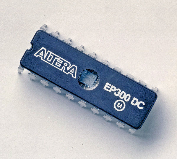
The 20-pin Altera EP300 was the company’s first product and the first UV-erasable PLD. Image credit: Altera
The EP300 became successful rather quickly and was soon followed by larger EP1200 and EP600 devices. Although they replaced PALs in many applications that did not require bipolar speeds, these devices did not directly compete with gate arrays, because they were too small. Gate arrays at the time offered ten times more logic capacity, and ASICs still lead by roughly the same amount.
Altera started selling the EP300 in 1984 and continued to develop larger and more complex CPLDs. Meanwhile, Xilinx sold its FPGAs, which also grew larger and more complex over time. Each company bad-mouthed the other’s approach to programmable logic. Altera’s CPLDs tended to win designs that needed deterministic speeds through the device and Xilinx’s FPGAs tended to win more complex designs that needed more registers. There was considerable overlap between the competing technologies.
This situation continued until 1992, when each company crossed the invisible FPGA/CPLD line. That year, Altera introduced the Flex 8000 programmable logic device family (although Altera refused to call these products FPGAs for a few years) and Xilinx introduced the XC7200 family of CPLDs, based on its acquisition of CPLD vendor Plus Logic. The two companies have remained arch competitors for almost four decades. Intel bought Altera in 2015, and AMD bought Xilinx in 2022. Still, the competition has continued.
Now, Intel is spinning out the programmable logic company that was once called Altera. The name of the new company will be announced on February 29. Whatever the new company’s name, you can expect that the fierce competition will continue, just as it has for the last four decades.
Acknowledgement: My thanks to Robert Bielby, who spent a few years at Altera and has an encyclopedic FPGA and CPLD memory.
References
Interview with Robert Hartman, 2018 September 11, Silicon Genesis: oral history interviews of Silicon Valley scientists, 1995-2022, Stanford University
Interview with Rob Walker, 1998 July 09, Silicon Genesis: oral history interviews of Silicon Valley scientists, 1995-2022, Stanford University
Interview with Paul Newhagen, 2019 November 18, Silicon Genesis: oral history interviews of Silicon Valley scientists, 1995-2022, Stanford University
Altera EP300 Design & Development Oral History Panel, August 20, 2009, Computer History Museum


Hi Steve. Thanks for the update on the history of the Programmable Solutions Group. If your readers want to learn about what comes next in this journey, they can tune in to our Vision Webcast on Feb. 29 at 9:00 am PST. Registration is at http://intel.com/leap.
Hi Steve, this is a great story about Altera from the founding days to 1992.
However, there is so much more to document about Altera from 1993 to 2014, when Intel closed the acquisition of Altera. So many great people, great innovations in programmable logic architecture and design software, many new generations of FPGA families, and of course the continued FPGA technology and market duopoly between Altera and Xilinx.
Misha Burich
Hi Misha. I agree. There’s a lot more history there. Some of it’s buried pretty deep, and someone will probably write it, someday. Meanwhile, check out Robert Bielby’s oral history at the Computer History Museum. There’s lots of Altera history in there. Some Xilinx history too.