

We’ve always been pretty impressed by Achronix – and for good reason. In an FPGA market where countless startups have tried and failed, Achronix somehow built themselves into a successful, independent, profit-making FPGA company. That’s not an easy task, and it required numerous “pivots” on the part of the company.
Initially, Achronix developed a family of novel asynchronous FPGAs and associated tools. When it became clear that engineering teams were not quite ready to buy into the asynchronous thing, Achronix developed a very market-savvy family of conventional FPGAs, with few novel features but with a clever mix of exactly right hardened IP that made the devices excel at specific targeted applications. Later, they switched fabs to Intel and released the world’s first Fin-FET FPGAs (yep – they beat both Xiliinx and Altera to that milestone, and theirs were the first modern FPGAs manufactured by Intel). Then, they pivoted again and went into the eFPGA business, selling the FPGA IP itself alongside their stand-alone chips. Each of those strategic moves gained more traction for the company, and the eFPGA line, in particular, drove some serious design wins and revenue for Achronix.
This week, Achronix is launching a new line of FPGAs with both a significant Moore’s Law boost (to 7nm TSMC) and some very interesting architectural innovations that should once again carve a chunk of hide out of their much-larger competitors (Xilinx and Intel). Once again, Achronix is “poking the bear” – going directly head-to-head with the dominant competitors in their most critical market segment, rather than flanking with a niche-market strategy like other small FPGA companies have done. The strategy is a bold one, and the combination of well-conceived devices and eFPGA flow availability will certainly score the company some prized socket wins.
Achronix says the new Speedster7t family is optimized for machine-learning and networking. The devices are manufactured on TSMCs 7nm FinFET process. Now that Intel owns Altera,, it probably wasn’t in anyone’s best interest for Intel to continue manufacturing new FPGAs to compete with their own. Given Achronix’s timeline, it seems likely that Achronix will be on a similar shipping schedule to both Intel’s recently announced Agilex devices (which are manufactured on Intel’s 10nm process – which is comparable to TSMC 7nm), and Xilinx’s long-awaited ACAP chips (also fabricated on TSMC 7nm). Of course, actual shipping schedules are difficult to divine, and shipping status is often obfuscated by company announcements, so we’ll have to see how the volume-shipment situation unfolds among the three companies.
The process technology picture puts the three companies more or less on an even playing field, so it will be architecture and tools that primarily differentiate the three vendors’ approaches and offerings. In the Achronix case, 7nm will bring a significant performance, density, and power-efficiency boost from their previous FPGA offerings. Going into production with their own 7nm devices using their new architecture will also work as a proof point for the company’s eFPGA line, as eFPGA customers will have a solid production run of the Achronix IP as a reference.
The interesting part of the Achronix announcement, however, is a set of significant architectural changes to the company’s FPGA architecture. First, like everyone else, Achronix is catering to the rapidly emerging AI and machine learning market, which spans everything from heavy-iron-cloud/data-center to low-power edge devices. AI inferencing, in particular, has much more specific and predictable data flow than typical general-purpose FPGA applications, so it is possible to gain significant efficiency by biasing the hardware architecture toward the needs of that particular computation problem. The key aspects of AI inferencing are massive convolutions, requiring matrix multiplication at a wide range of precisions (depending on the model). This runtime variability in precision is the fundamental reason that FPGAs excel at AI inference compared with fixed-width compute architectures. With an FPGA, you can reconfigure your hardware at runtime to be near-optimal for various-width data paths, whereas any conventional architecture will have to choose a bit-width or two and optimize around those.
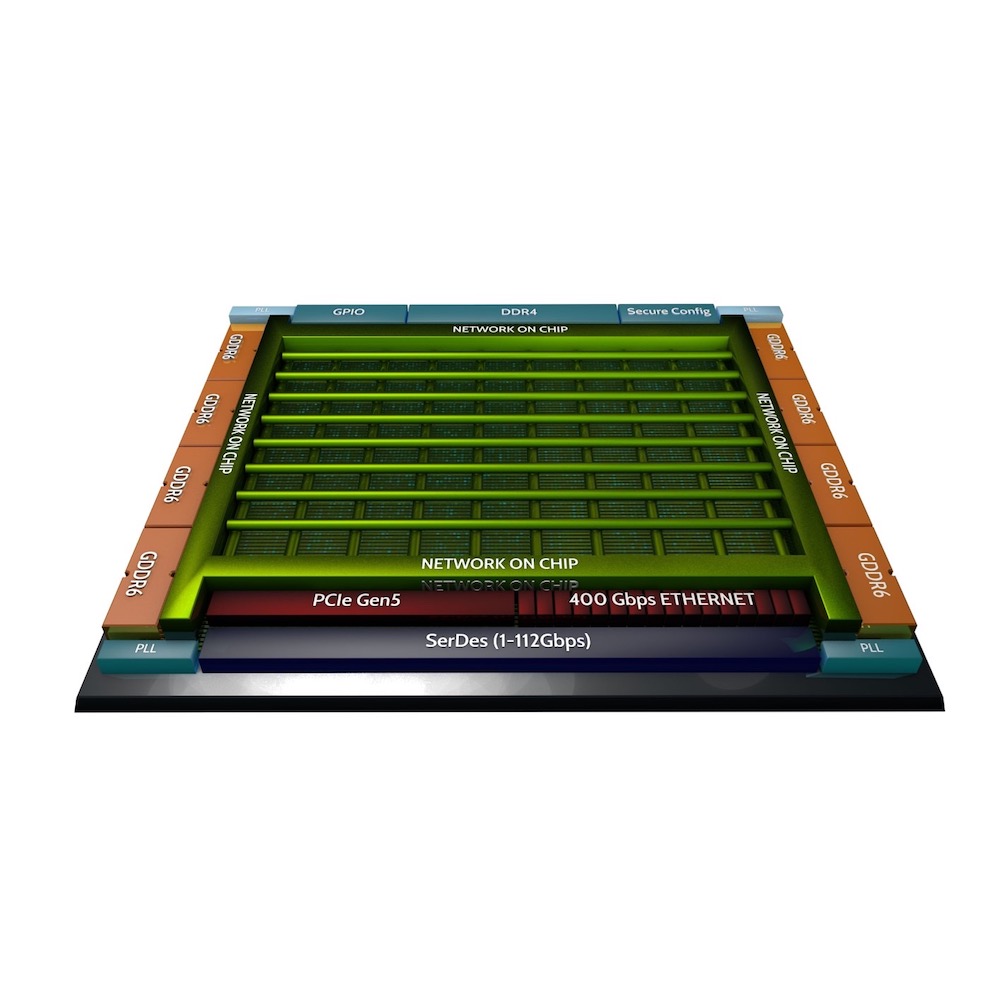
In order to attack this problem, Achronix took a three-pronged approach. First, they packed massive amounts of memory and IO bandwidth into the new devices. Second, they fundamentally overhauled the architecture of their logic cell. And finally, they overlaid a full-blown network-on-chip (NoC) over the entire device. Each of those innovations plays a key role in differentiating Speedster7t from competitive solutions. On top of that, the company’s eFPGA strategy provides a compelling reason for customers to choose Speedster7t if they plan to later bring the same functionality to market in an SoC of their own design.
Looking first at the memory and IO picture, Achronix made the interesting decision to go with high-bandwidth GDDR6 interfaces, rather than in-package high-bandwidth memory (HBM) or similar technology. The choice to go with GDDR6 keeps the cost down significantly, and, by building interfaces for off-chip memory, they allow the customer to choose what their particular application requires. Speedster7t devices pack up to 8 GDDR6 controllers, which could deliver an aggregate bandwidth of 4 Tbps. That means you could scale up to HBM bandwidths with a much lower cost, and, if you don’t need 4 Tbps, you can connect (and buy) just what your application needs.
On the IO front, Speedster7t can give you up to 72 transceivers that can operate from 1 to 112 Gpbs (PAM4). They also provide hard 400G Ethernet MACs with forward-error-correction (FEC), supporting 4x100G and 8x50G configurations. There are also hardened PCIe Gen5 controllers with 8 or 16 lanes per controller. In other words, you’ll be able to get the required data into and out of your processing engine, and into and out of memory.
Ah, but the bottleneck with FPGAs is often the on-chip routing fabric itself. As FPGAs get larger and larger – with increasing numbers of logic elements that need to be placed and routed – the need for dedicated routing resources grows faster than the other elements of the chip. The addition of ultra-high-speed SerDes interfaces exacerbates this problem. This is particularly challenging for FPGA companies because an increasing percentage of the chip has to be dedicated to routing versus active logic. If the FPGA company tries to skimp on the routing, they end up in the situation where most designs that try to use a significant percentage of the logic on the chip can’t be routed. This problem has famously bitten more than one FPGA vendor, with device families hitting the market that could be utilized only 60-70%.
On top of the problem of ballooning routing resource requirements, timing closure becomes increasingly challenging on giant FPGAs. With place-and-route runs requiring many hours, reaching timing closure on huge designs can be a major headache for designers. Achronix took the same approach to solving this problem as did Xilinx (in their upcoming ACAP architecture) – putting a full-fledged network-on-chip (NoC) overlaid on top of the conventional FPGA fabric. The NoC solves several problems at once. First, it gives very high-bandwidth connections between any logic elements on the chip that don’t have to go through the conventional routing resources and be subject to timing closure challenges. Second, it makes the entire design less vulnerable to locality issues, reducing the demands on placement and timing closure. The end result should be a design that is much easier to place and route and optimize, far shorter cycles to reach routing completion and timing closure, and much higher overall throughput.
Speedster7t’s NoC spans both horizontally and vertically over the entire FPGA fabric and connects to all of the FPGAs SerDes and memory interfaces. Each row or column is implemented as two 256-bit, unidirectional, industry-standard AXI channels operating at 2Ghz, giving a net 512 Gpbs of data traffic in each direction simultaneously in each row/column. Achronix claims that this gives their NoC about an order-of-magnitude more bandwidth than “competitive” NoC solutions (which we infer to mean Xilinx’s ACAP), but we are unable to either verify or disprove that claim. Regardless, the introduction of the NoC marks an entirely new generation of programmable logic technology. Interestingly, both Achronix and Xilinx share that sentiment, with Xilinx Marketing saying that the NoC makes their new devices not FPGAs at all, but a new category, “ACAP” on chip. Achronix is taking a more measured marketing approach, saying that the new devices are something like “FPGA+.” We tend to think of them all as just another new-and-improved generation of FPGAs.
The third pillar of Speedster7t’s re-designed architecture is a new machine-learning processor (MLP). The MLP represents essentially a re-thinking of the now-conventional FPGA structure where LUTs, block memory, and DSP blocks occupy distinct areas on the chip. Achronix combined new versions of all of these elements into new MLP cells. Each MLP is a configurable compute block supporting integer formats from 4 to 24 bits, as well as what the company refers to as “supercharged block floating-point format” that doubles the compute engines per MLP. The math blocks use high-density multiplier arrays with up to 32 multipliers per MAC block. This drives a variable-precision adder/accumulator, which gives Speedster7t a unique flexibility in handling various bit widths efficiently.
MLPs are tightly coupled with embedded memory blocks, eliminating the usual on-chip bottleneck with routing between block RAM, LUTs, and DSP resources. MLPs can operate at a frequency up to 750 MHz, and, because of the NoC, the locality of MLPs doing particular tasks is much less critical than with conventional architectures. That means that real-world designs are likely to see much closer to “theoretical maximum” TOps than with conventional FPGAs.
Speedster7t also includes a robust array of security features, including multiple layers of bitstream security. Keys are encrypted based on tamper-resistant PUFs (physically-uncloneable functions), and bitstreams are encrypted and authenticated by 256-bit AES-GCM. Bitstreams are also segmented, with separately derived keys for each segment, and the decryption hardware includes countermeasures against DPA (differential power analysis) side-channel attacks. On top of that, Speedster7t uses a 2048-bit RSA public key for activating the decryption and authentication hardware. Overall, this represents the most robust bitstream security regimen we’ve ever seen implemented in an FPGA.
The final arrow in Achronix’s quiver is their eFPGA option. Since the company is also in the FPGA IP business, customers who want to make a seamless conversion into an ASIC with their FPGA design can license the IP and harden key functions in the resulting ASIC, while keeping the FPGA programmability for functions that require in-system reconfiguration long-term. This is analogous to Intel’s eASIC flow, which allows hardening of FPGA-implemented functions. With Intel’s eASIC and their Agilex chips, you’ll be able to harden functions into eASIC chiplets and bond those chiplets to Intel FPGA chiplets in the same package. With Achronix, you’ll be able to license the FPGA IP itself and put the hardened blocks on the same monolithic device. Both approaches have their merits, and it will be interesting to see what customers do with each company’s capability. This is one area where Xilinx has yet to provide a similar option competitively.
The Speedster7t family includes 4 members ranging from 799K LUT4 equivalent to 2.6M LUT4 equivalent. On-chip memory ranges from 100Mb to 385Mb, and 112G SerDes transceivers range from 24 + 16 (LR + XSR) to 72 (LR). GDDR6 high-bandwidth interfaces range from 4 to 8, PCIe Gen5 from 1×16 to 2×16, and 400G Ethernet from two 4x 100G and one 8x 50G on the smallest device, up to eight 4x100G and four 8x50G on the largest device. Achronix says AI performance on INT4 ranges from 62 TOps on the smallest device to a whopping 416 TOps on the largest, and INT8 ranges from 21 TOps to 134 TOps. On ResNet-50, Achronix claims 8,600 images per second on their second-smallest device (7t1500) and 1,600 images per second on Yolov2.
Achronix says that tools supporting Speedster7t are available today, the AI/ML framework for TensorFlow, P4 Caffe2, will be available in Q3 this year, and the AC7t1500 devices and boards will be available in Q4. It will be interesting to see what kinds of design wins Achronix scores with this new offering, and what response it will generate from competitors Xilinx and Intel.


Wow … one very sweet pivot