


Just to make sure I have your attention, let’s start with the conclusion and then I’ll tell you how we got there. Is that OK with you? Good. In that case, the conclusion is that the clever folks at CacheQ have come up with a cunning solution that can take your regular single-threaded C/C++ code and compile it in such a way as to achieve multi-threaded acceleration on CPUs with multiple physical cores, all without any effort, pain, tears, trials, or tribulations on your part. Interested? If so, read on…
Let’s start with the fact that I love processors based on the von Neumann architecture — CPUs, MPUs, MCUs, and so forth (see also What the FAQ are CPUs, MPUs, MCUs, and GPUs? and What the FAQ are ASICs, ASSPs, SoCs, SOMs, etc.?). Having said this, although these processors are extremely clever, and while they are wonderful with regard to performing decision-making tasks, they tend to be horribly inefficient when it comes to accomplishing many data processing algorithms.
The problem in a nutshell is that these processors — and the high-level languages (HLLs) used to program them (e.g., C and C++) — are inherently sequential in nature, which means they plod along performing one simple operation after another. The reason these little rascals appear to be so fast and powerful is that we ramp up the clock rate, forcing them to perform hundreds of millions, or billions, of these simple operations each second. Unfortunately, the amount of power they consume rises as a square of their core clock frequency. As a result, you could easily get a first-degree burn by removing the heatsink on a CPU in a personal computer, workstation, or server and then touching that CPU (this would occur shortly before the system shut down and/or caught fire).
By comparison, the programmable fabric in FPGAs allows appropriate data processing algorithms to be executed in a massively parallel fashion, thereby allowing the same amount of processing to be performed using significantly lower clock speeds and consuming considerably less power, or dramatically increasing the amount of processing that can be achieved while consuming the same amount of power.
The obvious solution is to take the original C/C++ program, profile it to see where the bottlenecks are, and then partition things such that the slow and steady decision-making control code remains running in the CPU, while the fast and furious compute-intensive data-processing algorithms are dispatched to run on hardware accelerators implemented in an FPGA’s programmable fabric. Unfortunately, like most things, this sounds easy if you talk loudly and gesticulate furiously, but it’s a lot harder to implement than you might think. First, we are going to require some way to interface the software and hardware portions of the algorithm, where the type of interface we use (DMA, FIFO…) will be influenced by the profile of the data we wish to hurl around. Also, traditionally, the hardware accelerator in the FPGA would need to be implemented by an FPGA hardware design engineer. In turn, this meant the software and hardware folks were required to communicate with each other, which historically has not proven to be as efficacious as one might hope.
The ideal solution would be for a special software platform to perform the vast majority of the work, including taking the C/C++ source code, compiling it, profiling it, optimizing it, and partitioning it. This platform would then output those portions of the design that are to be run on the processor, along with those portions of the design that are to be run in the FPGA, where the latter would be in the form of a hardware description language (HDL), like SystemVerilog, that would be synthesized to generate a configuration file to be loaded into the FPGA. Oh yes, and this platform should also automatically generate any necessary interface software code and hardware logic necessary to allow the software and hardware to talk together.
All of which leads us to CacheQ. I first became acquainted with these guys and gals a couple of years ago circa 2019. At that time, they had come up with a solution to do everything we just discussed as illustrated below.
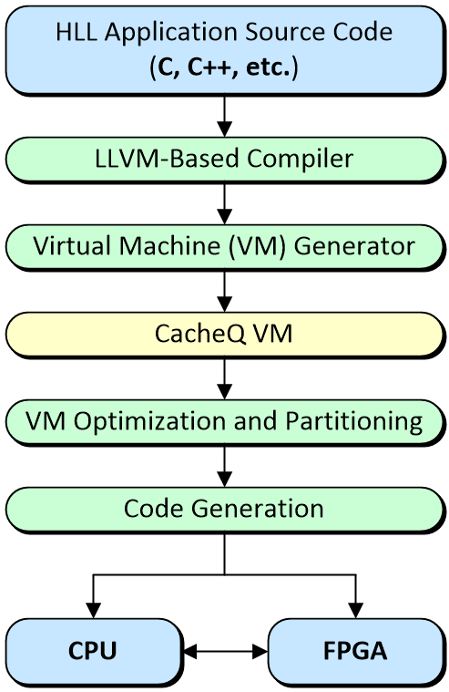
The CacheQ C/C++ to CPU + FPGA development flow
(Image source: Max Maxfield)
As I recall, their first-pass solution targeted desktop / workstation / server-class machines boasting X86 CPUs from Intel or AMD augmented with PCIe-based FPGA hardware acceleration cards supplied by FPGA vendors and others. Later, they added another string to their bow when they enhanced the system to include the ability to support heterogenous SoC FPGAs like Xilink’s Zynq devices, the high-end versions of which support multi-core Arm processors that communicate with programmable fabric by means of on-chip AXI busses. For example, the Zynq UltraScale+ MPSoC boasts dual or quad Arm Cortex-A53 cores, along with dual Arm Cortex-R5F cores, all augmented with humongous quantities of programmable fabric.
But Wait, There’s More!
Earlier, we alluded to the fact that some portions of our original C/C++ code may be optimally implemented by executing them in a sequential fashion on a traditional processor, while other portions of the code may be better served by realizing them in a massively parallel fashion in programmable FPGA fabric.
The thing is that there’s a third possibility. While some algorithms benefit from hardware acceleration, others may profit from running on multiple processor cores simultaneously. Now, remember that I’m a ruggedly handsome hardware design engineer, not a software development weenie, so please forgive any missteps in my terminology, but the idea is to take our single-threaded code and transmogrify it into a multi-threaded form that can take full advantage of multiple processor cores (these cores can be of the X86 flavor in workstations and servers, or they can be Arm or RISC-V cores lurking in embedded systems and skulking in FPGAs).
Traditionally, this has required a lot of work on the software developer’s part, including rewriting the code by hand, using special threading libraries, or employing complex parallel execution APIs such as OpenMP or MPI, which require the source code to be augmented by pragmas. Of course, it’s really embarrassing if you expend a lot of time and effort doing all this, only to come to the eventual realization that your code isn’t really suitable for multi-core processing in the first place.
Well, the clever chaps and chapesses at CacheQ realized that their tools already had the inherent ability to do all this for us. As a result, they recently announced support for multi-threading acceleration for CPUs with multiple physical cores through their new compiler, thereby offering software developers the ability to “write once, accelerate anywhere.” Equally valuable — if the code in question isn’t amenable to multithreading, the tool will tell you so. Even better, it will explain where the problems lie (data structures, indexing techniques…), because — if we’re lucky — it may be that some small tweaks will result in code that can be multithreaded.
This may be a good time for us all to feast our orbs on this short video in which we see the same original C/C++ application running on single thread compiled with gcc, then compiled to run on 1, 2, 3, and 4 threads/processor cores on a multi-core SoC FPGA. Finally, the exact same code is compiled using the exact same tool to run only in the FPGA’s programmable fabric.
I don’t know about you, but the fact that I can write some code knowing nothing about multithreading and then use CacheQ’s compiler and virtual machine to do all the threading for me — my only function (other than writing the code in the first place) being to specify the number and types of the processor cores — strikes me as being rather amazing.
And we are still only at the beginning of what’s possible. At the moment, for example, the options are (a) to take the original code and partition it into single-threaded code to run on a single processor core coupled with hardware accelerators implemented in an FPGA’s programmable fabric or (b) take the original single-threaded code and compile it into a multi-threaded equivalent that can take full advantage of multiple processor cores. If I were a betting man (“which, thank the Lord, I’m not, sir”), I’d wager it won’t be long before we see an option (c) that combines options (a) and (b). What say you? Do you have any thoughts you’d care to share on any of this?


I like these guys they have a lot going for them. Having said that they are comparing a slow arm to FPGA fabric. I do have questions. When running on the Arm did they use any of the vector units to do the calculation? Did they use the Neon GPU? How would this compare to one of the current x86 CPUs? What code base did they use? What compile options did they use for the Arm? A -O4 can make a world of difference.
A well designed Black Scholes IP runs at 180 Million transactions per second
http://www.kpubs.org/article/articleMain.kpubs?articleANo=E1ICAW_2013_v11n3_190
I have more questions but maybe they can respond to these?
Hi BCM — thanks for your post — let me “ping” them and ask them to respond — watch this space…
Hey Beercandyman,
Thank you for your questions and comments.
First, let me preface that I’m working on a follow-on video demonstrating the exact same experiment on a current x86 AMD Ryzen threadripper with 16 physical cores with hyperthreading that enables the use of of 32 logical cores as well as having a Xilinx Alveo U250 to demonstrate acceleration on x86 with an enormous Virtex Ultrascale+ VU13P. Please subscribe to our YouTube channel and stay tuned for that in the next few days. I’ll post a reply here and give Max a heads up when it’s available.
There is already a video on our channel showing a demonstration of just our new multi-thread compiler technology on x86, showing how to speed up the Black Scholes algorithm just by leveraging the multiple cores. In this video, I highlight the code used for the BS algorithm. We publish this code in our onboard repository of examples we give to customers to learn to use our tools and to replicate the results. This is currently a private repo as our company is currently scaling up our deployment so we have limited resources dedicated to making sure our customers are successful. Please contact us at sales@cacheq.net if you like to talk about evaluating our technology. In the meantime, here’s the other video I just referenced:
https://youtu.be/fpyv6M6sbKw
Next, direct answers to your questions. We did not use any of the vector units, nor did we use the GPU. We used straight-up gcc (the version that ships with Vitis/Vivado) with optimization level 3 (-O3). Beyond level 3, the compiler starts to make some non-standard math optimizations (eg -ffast-math etc) that may or may not be acceptable to the developer – ie you may start getting the wrong answer in floating point operations. We, or anyone can pass -O4 to both qcc and gcc if they are comfortable being that aggressive – we chose an apples to apples comparison to give a flavor for the tradeoff between single thread code, multi-thread code, and fpga acceleration – on an inexpensive FPGA typically used for embedded applications, which is a rather large market.
We selected Zynq to show a few things – one is the Cortex has 4 physical cores, which are largely underutilized to embedded developers – especially in Xilinx applications and it can be quite challenging to “partition” code and manually decide where to implement on the CPU and what to implement in the FPGA – and this is assuming people understand hardware and hardware description languages. This however is quite untenable for most software developers. The point being that parallelism can be extracted by a smarter compiler such as CacheQ QCC without the need for re-writing the algorithm to accommodate the hardware, and furthermore you can use the same compiler to seamlessly target heterogeneous accelerators. It would take someone months to years to figure out how to do that with HDL, OpenCL, or even HLS tools such as Vitis because you still need to code your C/C++ and architect the memory model manually to pass data to/from the accelerator. Our position is this is outside the skill set of most software developers – we can bring acceleration benefits without this overhead.
Our value-add is developer efficiency and ease of use. Could you hand-code an RTL implementation which might be more efficient? Perhaps. That is the same argument that used to be applied to people coding in assembly language instead of using a compiler – it will take you a very long time to prove that. This version of black scholes generates a bitstream for any number of FPGA targets from the same C in under an hour, with no hardware APIs, no OpenCL, no OpenMP, no HDL, not a single gate level simulation, no pragmas, no initiation intervals, no false sharing, nor synchronization techniques- just a more advanced compiler suite. Contact us for more info:
sales@cacheq.net
Thanks for the reply. I believe in most of what you said. You should understand that OpenCL implementations implement the whole standard and are very easy to use.
Cheers!
Steve
I’m afraid I cannot agree that OpenCL implementations are “very easy to use.” First of all, the major problem with working with heterogenous compute systems is making the architectural decisions as to what code will run on the host cpu and what will run on the accelerator. That literally is the thing people spend most of their time trying to decide h0w to efficiently (for performance) transfer the data necessary to accelerate an application, and this is incredibly non-trivial. You only have to start with the most basic of tutorials on OpenCL to quickly realize this. To perform something as mundane as a vector math operation, you can describe the kernel easily enough – but the host software side of the equation is a very low-level, driver-like code describing the process of instantiating memory buffers of specific sizes and manually moving data byte-by-byte. It is very low level code. Software developers cannot, and will not do this type of work – it is the realm of hardware engineers – and there are fewer, and fewer people willing to do this tedious work by the day. With CacheQ it is no longer necessary.
I cite this popular google result for an OpenCL tutorial. I really can’t see how anyone can review this code and claim it’s “easy” to use:
https://www.eriksmistad.no/getting-started-with-opencl-and-gpu-computing/
all this foolish chasing around…the answer is four point seven, but in the ancient Midorkan number system
Great post! How does this compare to, for example, OpenCL which can target cpu/gpu/fpga ?
OpenCL is a low level hardware API, that although technically C/C++, that does not make it easy to use, even for hardware savvy programmer. It looks like writing low level drivers. You must manually partition code, and write host-side software to communicate at the byte level to the accelerator as well as manually implement the accelerator kernel in the GPU, or FPGA. It is at best incredibly tedious to get basic things working, much less highly performant.
CacheQ QCC allows you to work completely in generic C, including memory allocation with malloc support and full understanding of all memory accesses and pointers. We are a dataflow compiler that builds highly pipelined, high performance accelerators with profiling, performance estimation, automatic parallesim, automatic or guided partitioning between the host cpu and accelerator – and most recently have added support for automatic parallel thread insertion for supporting homogenous multi-core cpus. You can compile in minutes with prediction of the accurate execution time on an fpga accelerator without ever generating the first line of HDL. We abstract all of the vendor tools away – no need to touch vivado, IPI, or HLS, and especially Petalinux if you are building for an embedded Arm on Zynq. We have high performance shells on Xilinx U250, U200, ZCU102, ZCU104, and Bittware VU9P based systems and can quickly get you up and working with any custom platform, and we are working to add support for Xilinx RFSOC, Intel FPGAs and nVidia GPUs so we are truly hardware vendor agnostic.
Contact us at sales@cacheq.net if you would like to have a deeper dive discussion.
As requested, below is a video demonstrating the same experiment from the Zynq MPSOC video, but targetting a high perfromance x86 CPU (AMD Ryzen ThreadRipper 16 core 3.4GHz) attached to a Xilinx Alveo U250 PCIExpress card (Virtex UltraScale+ VU13P device). As you can see everything pretty much scales with the clock frequency on the x86 and the story is the same. Acceleration is push-button, without the need for touching the source code – it’s a matter of changing the target platform from the zynq device to the Alveo card which runs roughly 5X faster than Zynq. No special APIs, no pragmas just pushbutton heterogeneous acceleration. The CPU multi-threading compiles in seconds, and the FPGA bitstream builds in just a few hours taking up approximately 70% of the fpga resources. Cool stuff!
Nice work. Thanks!