


Last week, I discussed the industry’s pursuit of Persistent Memory (PM) as a way to reduce mass storage (SSDs and HDDs) latency. (See “What Will Replace DRAM and NAND, and When?”) In that article, I mentioned some of the many candidate technologies in the PM Derby. Figure 1 is a graphic from Intermolecular (IMI) with a detailed list of PM technologies under development. The graphic shows the various candidate PM technologies and the important characteristics of each technology, including read/write latency, relative cell density and cell sizes (proxies for memory cost), the energy required to write a bit, write endurance, and an estimate of cost per Gigabyte.
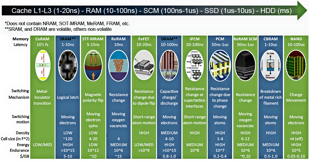
Figure 1: There are numerous candidate PM technologies, each with a unique mix of assets and liabilities. (Image Source: Intermolecular)
Here are some details for the candidate technologies. (Note that SRAM and DRAM are not candidate PM technologies; they’re included in the graphic just for reference.
NAND Flash EEPROM Memory: Invented in 1980, Flash memory is a block-oriented adaptation of nonvolatile EEPROM that has faster erase and write times and requires less chip area per cell compared to byte- or word-oriented EEPROM. Thus, Flash memory is cheaper and faster than EEPROM, and NAND Flash memory is, by far, the least expensive version of Flash memory, so it has become the memory of choice for SSD storage. The Flash storage mechanism employs two forms of electron tunneling, which stores or removes electrons on an FET’s floating gate, depending on whether a “1” or a “0” is being written. Although inexpensive, NAND Flash memory requires intelligent storage management to deal with the technology’s wearout failure mechanisms. These failure mechanisms cause bits in the memory to fail after as few as 100 write/erase cycles, so SSD vendors adopt wear-leveling and bad-block management algorithms to create SSDs that will last longer than a few days or months.
CBRAM (conductive-bridging RAM): CBRAM (also called “programmable metallization cell” or PMC) technology was originally developed at Arizona State University in the 1990s. A CBRAM memory cell’s state is determined by the presence or absence of a relatively low resistance across the cell’s two terminals. The existence of a filament between the terminals produces a low resistance state (LRS), while the absence of a filament results in a high resistance state (HRS). Filaments are formed (programmed) or dissolved (erased) in a thin film deposited between the memory cell’s two electrodes, and filament creation and destruction rely on metal ion migration.
ReRAM SCM (resistive RAM Storage-Class Memory): ReRAM is based on a device called a memristor, a previously mythical beast originally conceived by circuit theorist Leon Chua in 1971. Chua was simply filling in a two-by-two grid of two-terminal devices exhibiting specific current/voltage behaviors including the thoroughly familiar resistors, capacitors, and inductors. A memristor’s electrical resistance depends on the history of the current that has flowed through the device, and memristors were purely theoretical until HP Labs managed to fabricate one in 2008 using a titanium dioxide thin film. In Figure 1, the chief difference between ReRAM SCM and ReRAM appears to be cell size, which largely seems to affect cost.
PCM (Phase change Memory): PCM exploits the resistance change caused by a thin-film material’s transition from a crystalline form to an amorphous form. The two phases (crystalline and amorphous) exhibit different resistances. Early PCM was based on thermally inducing phase transitions in chalcogenide glass thin films. Later prototypes have been based on thin-film chalcogenide alloys that combine germanium, antimony and tellurium (GeSbTe, called GST for short). GST exhibits better thermal stability than chalcogenide glasses.
iPCM (interfacial Phase-Change Memory): The difference between iPCM and PCM is that an iPCM memory cell does not use heat to induce a phase change. Some other form of excitation is used to cause a state transition in the iPCM thin-film storage media. One such excitation source is a laser.
FeFET (ferroelectric FET): Ferroelectric RAM (FRAM) has been around since the 1980s and is used today in limited applications such as small, non-volatile memories in microcontrollers. But FeFET memory is not FRAM. The old FRAM designs were based on ferroelectrically induced changes in a capacitor’s thin-film dielectric. However, capacitors don’t scale well; Moore’s Law died for them a long time ago, so FRAMs have been stuck at the 130nm node. You won’t be building large memory arrays at that node. In the newer FeRAM design, the ferroelectric thin-film dielectric forms the gate insulation for nicely scaling FETs. The ferroelectric material can be in one of two stable states that depends on the position of certain atoms in the thin film. An electrostatic field moves the atoms within the thin film, and the material remembers its last state after the external field is removed. The different states have different resistances. (Ferroelectric Memory Company (FMC) uses hafnium oxide for the dielectric material.)
ReRAM (resistive RAM): See ReRAM SCM.
STT-MRAM (spin torque transfer magnetic RAM): In a callback to the days of magnetic cores, STT-MRAM induces magnetic states in thin-film magnetic material. Magnetic polarization of a free magnetic layer, compared to an adjacent, magnetically pinned layer, produces a two-state MRAM cell. The two magnetic polarization states have different resistance.
CeRAM (correlated electron RAM): CeRAM is based on a thin film consisting of a transition metal oxide like nickel oxide. Storage is based on a reversible metal-to-insulator transition through oxidation and reduction (the loss and gain of an electron) at a single atomic site. The state change in the material produces a large change in the cell’s resistance.
One Common Thread
The common thread for all of these PM technology descriptions is the phrase “thin film.” All of these PM technologies depend on a variety of physical attributes in a thin-film materials menagerie. Taming this menagerie requires a thorough electrical characterization of each thin film based on material composition, layer stack, thickness, surface treatment, and many other factors. There’s still a lot of research to be done with respect to the materials science of these PM thin-film candidates.
In the days of vertically integrated device manufacturers (IDMs), this type of research would have been done exclusively at the IDM’s own semiconductor research facilities. However, research costs money (in the short term) and production makes money, so most device manufacturers prefer to use their clean-room space for high-volume production, which creates a niche for a research fab.
Enter IMI, a small fab located on San Jose’s North First Street, that specializes in materials and process research instead of production. I visited IMI’s facility recently, donned a bunny suit, and toured IMI’s 45,000-square-foot fab (see Figure 2).
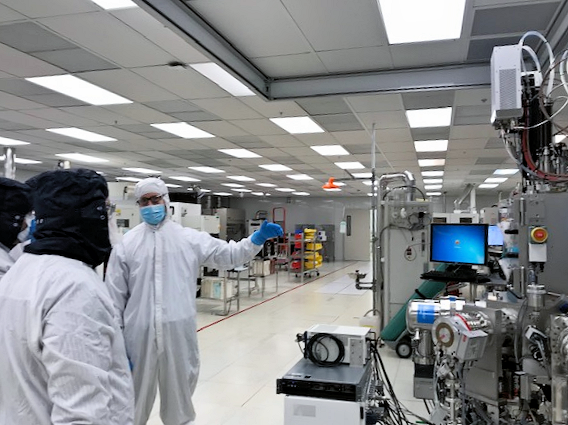
Figure 2: A visit to IMI’s research fab.
This wasn’t my first visit to a fab, and one thing immediately became obvious after my group suited up and entered the clean room: there’s no lithography going on here. (My first clue: a distinct lack of yellow light and yellow windows.)
Say what? What good’s a fab without litho?
It’s all about the deposition, no (very little) litho
IMI’s fab is filled mainly with two types of tools: PVD (physical vapor deposition) tools and ALD (atomic layer deposition) tools. These are the two main tools you need to apply thin films to silicon substrates. IMI has designed multiple generations of its own PVD and ALD tools specifically to support thin-film materials research. In addition to the PVD and ALD tools, the company maintains a complex metrology lab inside its clean room to characterize the deposited films.
Instead of using lithography to define where the films are deposited on the wafers, IMI uses physical apertures (essentially they’re metal stencils) for PVD deposition. Special showerheads in the ALD chamber enable quadrant-based ALD deposition, as shown in Figure 3, which permits PVD spots and ALD quadrants to be combined on a test wafer.
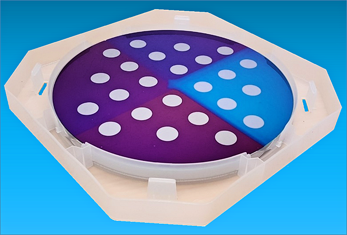
Figure 3: Stenciled PVD deposition lays down circular spots of thin film, and IMI’s ALD tools lay down film quadrants using specially configured shower heads. (Image Source: IMI)
IMI’s PVD tools can deposit multiple, different thin films on as many as 36 spots per wafer. As many as four sputter sources can supply material for each PVD thin-film layer. Each ALD quadrant can also deposit different material combinations on the wafer. Multi-layer PVD capability, combined with the four ALD quadrants, allows IMI to run more than 100 thin-film materials experiments per wafer – one per spot – which both reduces the cost of each experiment and allows more experiments to be run per unit time.
For example, IMI tested 75,000 different conditions over a two-year period in one experiment series. When you and your competitors are racing to find the best thin-film composition to achieve or optimize a specific electrical characteristic, the ability to run a lot of experiments quickly is what’s going to win the race.
Instead of volume manufacturing, IMI’s fab is focused on high-throughput experimentation.
The semiconductor industry spends a lot of time and energy getting excited about the latest lithographic breakthroughs. Case in point: after twenty years of reporting on the “excitement” of EUV lithography, we’re finally almost ready to start using EUV in production fabs.
Materials science is no less important, especially for PM technology research. There’s a lot more to the art and science of chipmaking than wrangling silicon these days. We’re throwing more than half of the periodic table around in the fabs, and the semiconductor world inside of the fab is getting only more complex.


