

Long, long ago, back when Richard Nixon was president of the United States of America, magnetic cores were the dominant computer memory technology. In fact, magnetic cores were essentially the only practical memory technology for two decades. Although we had hand-woven rope memory for ROM, only the Apollo space computers and the HP 9100 desktop calculator used it. My 1954 “Britannica Book of the Year”—a real book, made from dead trees—says that RCA Laboratories announced a working core memory in 1953 that used a 100×100 grid of wires to control 10,000 ferrite toroids.
Jay Forrester’s Project Whirlwind team at MIT also developed a magnetic core memory that was first used in the groundbreaking, real-time Whirlwind computer around the same time as RCA’s announcement. Magnetic core memory quickly became the memory of choice for mainframe computers (and eventually minicomputers), tipping mercury delay lines (derived from World War II radar technology) and CRT-based electrostatic memories onto the great scrap pile of memory history.
Magnetic core memory quickly swept away these other two memory technologies, largely for two reasons: magnetic core storage was relatively fast, but, just as important, it was persistent. You could cut the power to a properly designed magnetic core memory and, when you flipped the power switch back on, all of the stored bits would still be exactly where you left them in memory. In the mainframe and minicomputer era, magnetic core memory usually functioned as both ROM and RAM.
Then, in 1970, Intel let the serpent into magnetic core’s Garden of Eden by announcing the industry’s first DRAM, the 1103, which actually managed to work somewhat reliably a year later, after the chip’s fifth stepping. Intel had been founded in 1968 for the express purpose of replacing magnetic core memory with semiconductor memory. Magnetic core memory was hand-woven, mostly by women with steady, small hands, sharp eyesight, and buckets of patience. Memory vendors never succeeded in automating the manufacturing process for magnetic core planes.
Bob Noyce and Gordon Moore founded Intel to throw the nascent integrated circuit mass-production technology they’d developed at Fairchild at core memory’s speed, capacity, and cost limitations. Intel’s 1103 DRAM was born ready to ride the Moore’s Law rocket sled, and DRAM has now been King of Memories for nearly half a century. Despite not being persistent, DRAM is inexpensive and it’s fast.
We use EEPROM for nonvolatile semiconductor storage, particularly NAND Flash EEPROM because its cost per bit is relatively low and because it’s persistent. However, storing data in NAND Flash memory is also relatively slow.
Jim Pappas, Intel’s Director of Technology Initiatives, emphasized NAND Flash memory’s speed problem during his presentation titled “Why Persistent Memory Matters,” which he presented as a member of the “Good Monsters—Emerging Memory Technologies” panel at the recent Storage Visions 2018 conference held at the Hyatt Regency hotel in Santa Clara, California.
And just what is Persistent Memory (PM)? The cynical answer is that it’s the latest, au courant name for storage-class memory—the memory that’s supposed to sit between DRAM and Flash in terms of both speed and cost per bit. However, I guess we’ve become conscious of being class conscious and so this new type of memory apparently needed a new name.
A more technical answer is that PM is memory that’s nearly as fast as RAM and much faster than NAND Flash memory, but, like NAND Flash, it’s also nonvolatile and much less costly than DRAM on a per-bit basis.
Here’s a chart presented by Tom Coughlin and Jim Handy at SNIA’s Storage Developer Conference this year. (SNIA is the storage Networking Industry Association.) The chart nicely summarizes the memory hierarchy slot (a bright blue circle) being targeted by PM, plotted as bandwidth in megabytes per second versus price per gigabyte on a log-log scale. Note that in this chart, the blue circle is marked “3D XPoint” but it’s roughly the same region being targeted by all PM technologies.
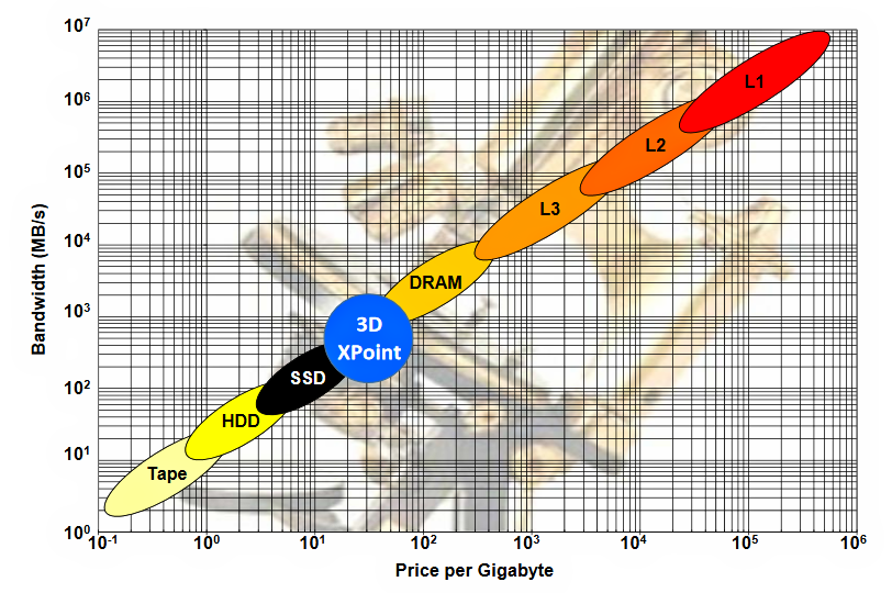
Figure 1: Persistent Memory (PM) will occupy the price/bandwidth gap that sits between DRAM and NAND Flash storage. PM occupies the blue circle, which shows 3D XPoint as a placeholder for all PM candidate technologies. (Chart from Coughlin & Handy PM presentation at SNIA SDC 2018.)
There are many candidate technologies for implementing PM including MRAM (magnetic RAM), ReRAM (resistive RAM) and CBRAM (conductive bridging RAM), FeRAM (ferroelectric RAM), and PCM (phase-change memory), just to name a few. To succeed, any candidate technology trying to worm its way into the memory/storage hierarchy needs to provide more bandwidth than the technologies below it and must cost less per bit (or gigabyte) than technologies above it on the chart.
There are many candidate memory/storage technologies for the same reason that there are so many horses in the Kentucky Derby: one of them is bound to win. Although the outcome’s far less certain in the PM Derby, there’s lots of money to be made if any one of these technologies manages to mature into an economical, manufacturable process.
In his Storage Visions presentation, Pappas first acknowledged that humans have a difficult time mentally connecting computer-scale time periods (microseconds and nanoseconds) to the human scale (seconds, minutes, hours, and days), so he used the image in Figure 2 to provide visceral contrast between the latencies of PM and storage.
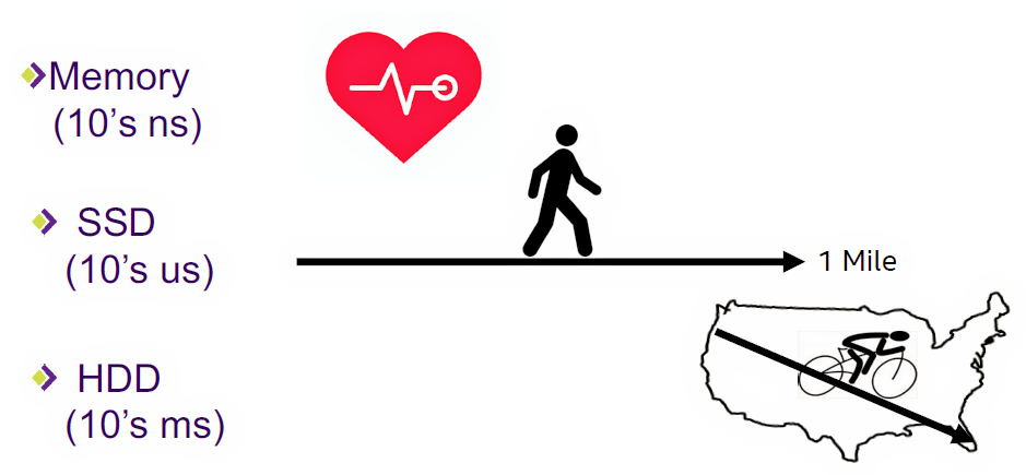
Figure 2: Slowing memory speeds to human speeds underscores just how slow storage devices are. (Image Source: Jim Pappas, SNIA, and Intel)
Imagine that DRAM latency is one second. (Normally, it’s on the order of tens of nanoseconds.) We all carry an internal, one-second reference clock. It’s our heartbeat. Assuming that one second is the baseline time scale, then an SSD satisfies a data request in the time that it takes you to walk a mile. That’s a lot of heartbeats, ignoring the affect this walk has on your heart rate. Using this same expanded time scale, you have enough time to ride a bicycle from Intel’s campus in Hillsboro, Oregon to Miami Beach while waiting for a hard disk drive to satisfy a data request.
This simple analogy underscores existing storage technology’s chief vulnerability: It’s much, much too slow compared to processor speeds. Figure 3 provides a more technical assessment of storage and PM memory latencies.
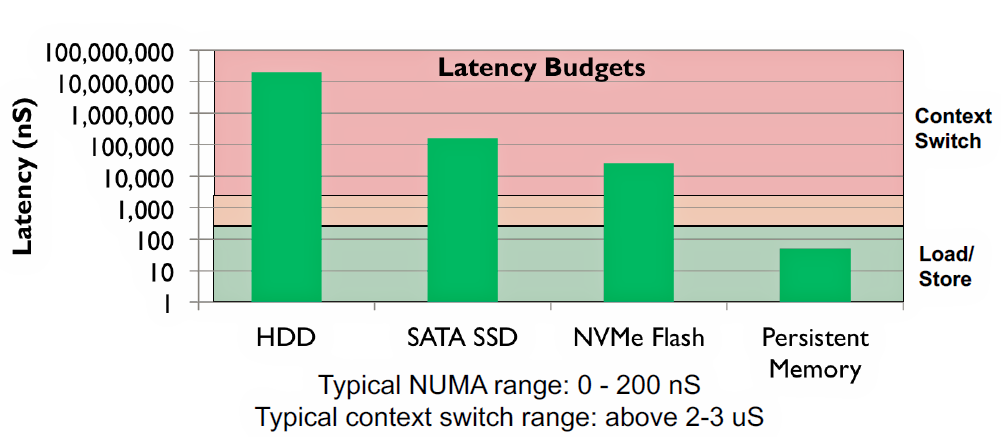
Figure 3: The load/store threshold at around 200 nsec differentiates memory from storage. (Image Source: Jim Pappas, SNIA, and Intel)
Note that storage devices (HDDs, SSDs, and NVMe Flash memory) all fall into the pink zone. That’s the slow zone. That’s the zone that’s sooooo slow, the processor’s simply not going to hang around waiting to get a response for a data request. In Figure 3’s pink zone, it’s more efficient for the processor to switch context and start another task during the time the computer’s storage subsystem needs to fulfill the storage request.
A hypothetical PM technology with a data latency of less than 100 nsec falls into the load/store region in Figure 1. If you develop a fast, bulk-memory technology—a memory technology that can respond with a latency of only a couple of hundred nanoseconds—then the processor is better off waiting for the data request to be fulfilled, because context switches require two to three microseconds, which is much longer than the wait time and therefore much less efficient. Using context switching to mask storage latency simply makes no sense when PM is present.
There will be still other reasons for using context switching, however, but the addition of PM to the memory/storage hierarchy would seem to have some interesting and positive implications for multicore processor architectures as well. If the need for context switching diminishes because of the presence of PM, then it seems to me that the use of more processor cores to run simultaneous applications might well surge, to further reduce the percentage of processor time wasted on context switches. It’s a possible future virtuous cycle for software architecture.
According to Pappas, PM’s additional speed will ultimately disrupt the fundamentals of computer design, but not immediately. It will do so in three evolutionary stages. SNIA calls these stages “Horizons,” as shown in Figure 4.
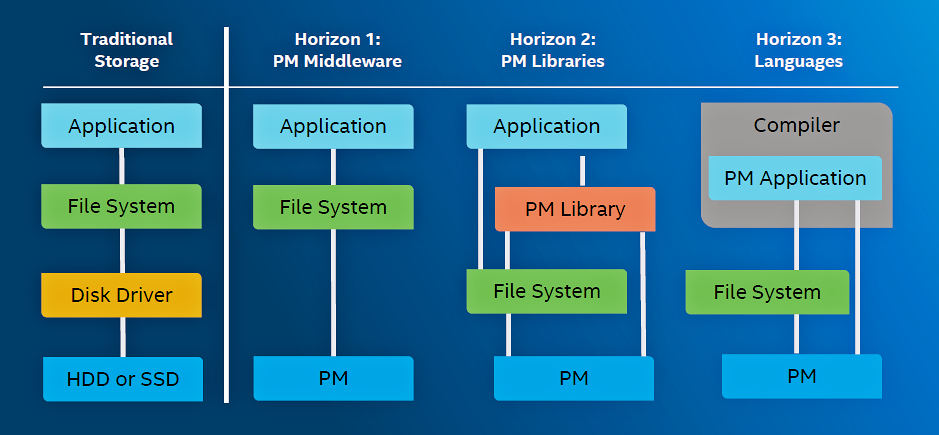
Figure 4: SNIA says that PM will be adopted in three stages. (Image Source: Jim Pappas, SNIA, and Intel)
The existing file system architecture and hierarchy appear on the left in Figure 4. The application makes a request of the file system, knowing that the data it seeks isn’t in main memory. The file system translates the application’s data request into multiple calls to the software disk driver, which results in the eventual retrieval of the data from the storage hardware. The file system and disk driver are software gaskets, used to adapt the hardware processor’s high speed to the disk drive’s slow latency, which is glacially separated from the processor’s load/store region.
For the last half century, applications don’t talk directly to storage systems; they make requests through the operating system’s file system, which effectively insulates the application running on the processor from the mechanics of the storage hardware. This compartmentalization makes it possible to replace the software disk driver and the hardware storage device with PM middleware and PM hardware, as a first step in the evolution of PM-based computer architecture.
Note that we’re already seeing this start to occur. In this first evolutionary step, an application accesses data stored in PM through the existing file system. This first step replaces slow storage with faster PM.
Although Pappas was careful not to overly favor one candidate PM technology over another in his presentation, his employer, Intel, introduced and started shipping Optane DC PM DIMMs back in August. (See “The New, New Intel Unleashes a Technology Barrage.”) These Optane DIMMs plug into DDR4 memory slots on an Intel Skylake motherboard and make the Optane PM directly accessible to the processor. (Note: Optane PM DIMMs are not quite as fast as DDR4 SDRAM DIMMs, so a compatible memory controller is also required.)
Even though the processor has direct access to the Optane memory space, existing applications are written to access storage through the file system, which explains this first evolutionary step. The applications must be rewritten to take full advantage of the Persistent Memory. (SNIA will be creating a “center of excellence” for PM applications next year.)
That brings us to the column marked Horizon 2 in Figure 4. In the evolutionary stage that SNIA calls Horizon 2, the file system remains for backwards compatibility, but a PM API library has been added so that new applications can use API calls to directly address data stored in PM. Such accesses through these API calls will be far faster than accessing data through the file system, so the Horizon 2 evolutionary step provides a speed advantage over Horizon 1.
In the final stage, called Horizon 3 by SNIA, the operating system directly incorporates PM APIs, and compilers use them to directly access data stored in PM attached to the processor bus. How soon will this happen? Linux, Microsoft Windows, and VMWare have all incorporated PM APIs already, according to Pappas. The latest Java Virtual Machine (JVM) has also incorporated built-in PM APIs, so any Java application can now access PM as well.
SNIA will be holding a PM Summit on January 24, 2019 in the same Santa Clara Hyatt Regency hotel that hosted Storage Visions 2018. The event is free. PM Summit underwriters include Intel, Smart Modular Technologies, AgigaTech, OpenFabrics Alliance, Netlist, and Viking Technology. If you decide to attend, be sure to thank them for getting you into SNIA’s PM Summit for free.


The Load/Store times are somewhat misleading, high-density memories on the end of serial links (PCIe) are not that fast on small transfers. If you want that speed you’ll have to do PiM – die-stacking the memory with CPU. Likewise using a single cache-coherent data-bus becomes the throttle on the entire system.
The next level in performance needs a new architecture – https://youtu.be/Bh5axlxIUvM
Note: L1 cache is expensive because most of it is not memory, a CPU with just plain static memory or PM (say 64k-words) is super fast and fairly cheap per byte, folks have just gotten used to all the caching and pipelining and forgotten how much latency all that adds.