

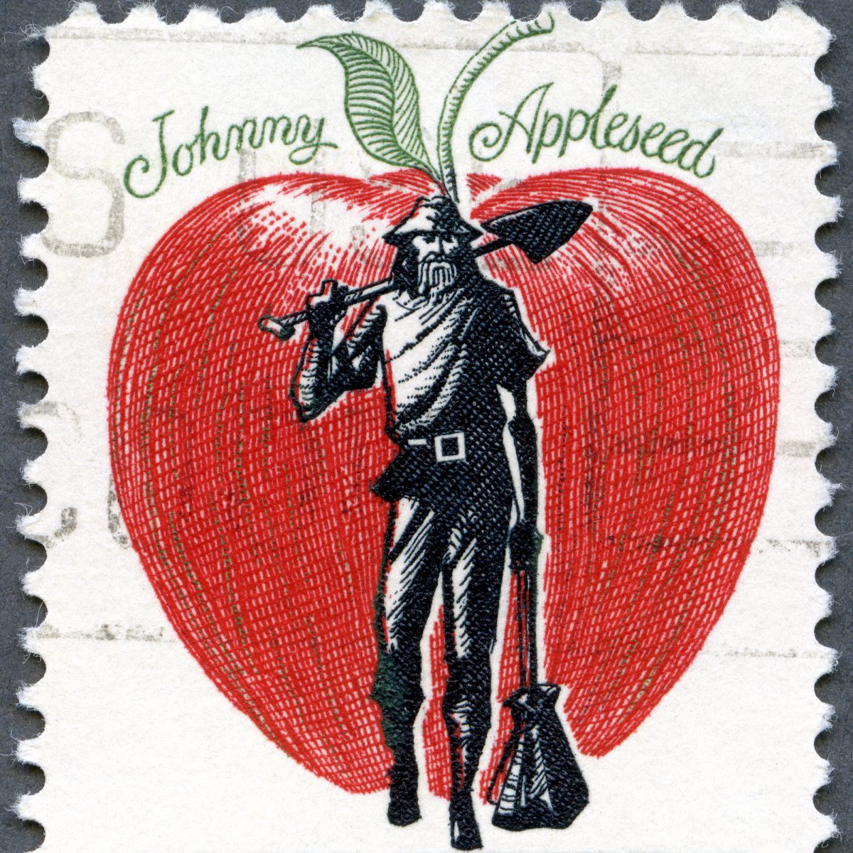
It’s hardly surprising that semiconductor companies were reluctant to invest much energy into MOSFET development in the early 1960s. Early MOSFETs were 100 times slower than bipolar transistors, and they were considered unstable, for good reason: their electrical characteristics drifted badly and unpredictably with time and temperature. A lot of research and development work would be needed to transform MOSFETs into reliable electronic components. However, when Fairchild Semiconductor hired Frank Wanlass, the MOSFET found its champion. Wanlass was committed to the MOSFET, not to any company. He went anywhere and did anything he could to promote the MOSFET’s development. He became the Johnny Appleseed of MOS (metal-oxide-semiconductor) technology, freely planting MOSFET seeds, whenever and wherever.
Fairchild hired Wanlass in August 1962 after he received his PhD in physics from the University of Utah. He’d become interested in MOS technology when he read about RCA’s work with thin-film cadmium-sulfide (CdS) FETs while studying for his doctorate in solid-state physics. The simplicity of the FET device structure first intrigued and then obsessed him. He realized that the FET’s simple structure meant that many FETs would fit on a semiconductor die, and he conceived of building complex integrated circuits (ICs) using these devices. But RCA’s thin-film CdS FETs were far too unstable. Even when left on a shelf for a few hours, their electrical characteristics drifted dramatically. Wanlass thought that making FETs with silicon instead of CdS would solve the parametric drift problem. He was wrong, as it turns out. Semiconductor FETs suffered from drift for several years until the MOS manufacturing process could be sufficiently cleaned to eliminate the contaminants that caused FET parametric drift.
When Wanlass joined Gordon Moore’s Research and Development group at Fairchild, the company had a policy of letting new PhD hires work on any project they cared to undertake. Wanlass decided to focus on MOSFETs, even though Moore’s department wasn’t especially interested in making the devices. However, Moore’s department was vitally interested in MOS processing, because that was the basic structure and nature of Jean Hoerni’s planar manufacturing process, which Fairchild used to make bipolar transistors and ICs. Any increased understanding of the planar process and any improvements made to the process technology would further Fairchild’s ability to manufacture bipolar transistors and integrated circuits.
Wanlass wasn’t interested in studying or analyzing the characteristics of the MOS process. He wanted to fabricate discrete MOSFETs, build ICs with MOSFETs, and design system-level circuits using those devices to nurture demand for the components. Over the next year, he did exactly that. In less than six months, Wanlass designed and fabricated individual p- and n-channel MOSFETs in silicon using the planar process. All the p-channel devices exhibited severe parametric drift, while none of the n-channel devices worked at all. He tested the parametric drift of p-channel devices by putting them in a curve tracer and heating them with a cigarette lighter. He then designed and fabricated a flip-flop IC using MOSFETs and achieved an incredible wafer yield of better than 80%. He developed application circuits for MOSFETs including a current meter that exploited the MOSFET’s extremely high input impedance.
Along the way, Wanlass and his manager C.T. Sah patented the idea for CMOS circuits, which combine p- and n-channel MOSFETs on one silicon die. CMOS is the foundational transistor technology for nearly every IC now manufactured. (Note: Sah is often listed as the sole inventor of CMOS, but his name is on the patent because he was Wanlass’s manager, and it was customary to list the manager along with the inventor on the patent application.)
In early 1963, Gordon Moore started hiring more people to more thoroughly analyze MOS process technology. However, he wasn’t interested in studying MOSFETs. He simply wanted to better understand the metal-oxide-semiconductor planar process so that Fairchild could make better bipolar transistors and ICs. The analysis team became Bruce Deal, Andrew Grove, and Ed Snow. They weren’t put on a formal team, but they soon discovered each other and their complementary assignments through casual office interactions. Deal worked on oxidation and surface states. Snow analyzed MOS transient instabilities. Grove wrote programs to model the analyses.
By late 1963, Wanlass was certain that Fairchild wanted only to study and analyze MOS devices, not build them commercially, and he much preferred making devices, not studying them. Wanlass left Fairchild in December 1963, just one year and four months after he joined the company. He took a position with General Microelectronics (GME), which had been started by a small group of former Fairchild employees who had decided to form a semiconductor company. GME was one of the earliest Fairchild Semiconductor spinoffs, known collectively as the Fairchildren. GME’s goals and direction clearly would take Wanlass where he wanted to go, and Wanlass instantly took charge of creating and fabricating MOS transistors and ICs.
Wanlass brought his well-developed MOS design skills to GME. He’d successfully built MOSFETs and small MOS ICs at Fairchild, so he brought those capabilities, but he also brought one other important thing. While working at Fairchild, Wanlass discovered that he could significantly reduce the time and temperature drift of MOS characteristics if he evaporated aluminum interconnect on the semiconductor wafer using electron-beam vaporization instead of thermal evaporation. Fairchild had been building electron-beam evaporators in its basement. It was one of the first semiconductor companies to have this type of evaporator on hand.
In an interview, Wanlass said, “I was driving down the 101 freeway one day, on a Sunday, and it hit me. It’s got to be sodium, and I had sent out some aluminum wire to be spectroscopic analyzed. I knew from my college work, some of my thesis work, that sodium… I knew for a fact that sodium, with just a little help from temperature and voltage, would diffuse right through quartz. It had a very high diffusion quotient. I knew that. That was from experiments in college.”
Suspecting that the thermal vaporization process somehow deposited contaminated aluminum on the semiconductor wafer and that this contaminated aluminum was causing devices to drift, Wanlass tried evaporating platinum onto the wafers instead of aluminum. There’s no chemical etch for platinum, so he had to scribe the gate electrodes in the platinum layer by hand using a pointed tungsten probe. The resulting MOSFET didn’t drift nearly as much. He then tried using gold and other metals, but platinum was superior. Then, for completeness, Wanlass used the electron-beam evaporators to put aluminum on a wafer. They also didn’t drift nearly as much, and electron-beam evaporation of aluminum quickly became part of the MOS process recipe. This all took place while Wanlass was still at Fairchild, and he brought this important knowledge to GME.
Eventually, the industry would understand that sodium ion contamination causes drift and kills p-channel MOSFETs over time, while making it impossible to build working n-channel MOSFETs. The aluminum was being contaminated with sodium when it was drawn through wire dies to make the aluminum wire that served as the feed stock for the vapor deposition. The wire dies were lubricated with sodium. Electron-beam vaporization employs a shutter mechanism that shields the wafers from the crucible of molten aluminum until the aluminum reaches its evaporation temperature. Sodium has a much lower boiling point than aluminum, so the sodium boiled off and dissipated before the shutter in the evaporation chamber opened and exposed the wafer to the aluminum vapor.
Wanlass used electron-beam evaporators to metallize wafers at GME, and by May 1964, he’d produced a working, discrete MOS transistor. The company introduced this device commercially months before Fairchild could do the same. Wanlass then built a 20-bit shift register as a monolithic MOS IC, not because customers demanded it, but simply because he could. A 20-bit shift register made a terrific MOS IC demonstration vehicle. At the time, shift registers were the industry’s preferred form for small digital memory devices because of their low pin count, while allowing the devices to be mounted in a TO-5 metal-can transistor package, with as many as 12 pins.
Although GME had a booth on the show floor at the 1964 WESCON (Western Electronic Show and Convention) held in Los Angeles, the company also rented a hotel room just to show Wanlass’s shift-register IC. GME’s MOS shift-register IC demo impressed prospective customers, firmly established GME’s leadership in MOS ICs, and positioned Wanlass as the industry’s leading authority in MOS IC development.
GME’s MOS shift-register IC demo, the company’s growing reputation as a MOSFET vendor, and the salesmanship and connections of retired US Marine Colonel Art Lowell, one of GME’s founders, drew customers from the US government. The company’s first MOS design contract was with NASA, to design an IC with six or seven MOSFETs for the Interplanetary Monitoring Platform spacecraft, a program that was managed by the NASA Goddard Space Flight Center in Greenbelt, Maryland. Spacecraft have severe power restrictions, so low-power MOS ICs seemed made to order for the project. The super-secret National Security Agency (NSA) also became an early GME customer. The NSA had an ambitious plan to put wireless communications with decryption circuitry into soldiers’ helmets, recalls Wanlass.
Device density led GME to take the path leading to the MOS IC’s early destiny: calculators. GME signed an agreement with Victor Comptometer to build a MOS calculator chipset consisting of at least 20 ICs, each containing hundreds of circuit components including MOSFETs. This should have been a dream project for Wanlass, but he could see that GME would not be up to this challenge. Wanlass left GME in December 1964 with the calculator project just beginning. As he’d expected, GME’s calculator project was beset by delays. The company started to have money problems and was acquired in 1966 by Philco-Ford. It became Philco-Ford’s Microelectronics Division, and the General Microelectronics brand ceased to exist. Philco-Ford finally ditched the Victor calculator project in 1968, and the company itself ceased to exist a few years later when Ford decided to sell it off. “GME went out of business because they didn’t have enough money and they were pushing too fast, too soon,” said Wanlass during an interview.
When he left GME, Wanlass and four of his colleagues first tried to start their own semiconductor company, but the deal fell through. Instead, the team joined General Instrument (GI), an east coast electronics conglomerate that wanted to add semiconductor manufacturing, specifically IC manufacturing, to its portfolio. GI had already hired managers from other semiconductor makers including Philco and IBM. Adding Wanlass and his team set the new semiconductor division’s direction: MOS.
The first thing that Wanlass did at GI was to design and fabricate a 21-bit shift-register IC, one bit larger than GME’s device, so that GI could claim to have the biggest. Soon, GI introduced 50- and 90-bit MOS shift register ICs. Then, something Wanlass did during his tenure at GME came back to him with a return on his investment. While Wanlass was demonstrating GME’s 20-bit shift register in that hotel suite at WESCON in 1964, he met an engineer named Bob Booher who was working for Rockwell Autonetics, an avionics contractor known especially for developing inertial guidance systems for US submarines and ICBMs. Wanlass seems to have infected Booher with his zeal for MOS ICs during that meeting.
A couple of years later, Booher found Wanlass at GI and asked if GI could fabricate a chip he’d designed. It was a Digital Differential Analyzer (DDA), and it was a very ambitious device for the era. Booher’s DDA was a digital implementation of Vannevar Bush’s Differential Analyzer, a mechanical analog computer used extensively for solving differential equations numerically before the advent of digital electronic computers. Eventually, Rockwell Autonetics would start its own semiconductor manufacturing group, but that was in the future, and Rockwell was unable to make such a large chip at that time. The chip design required a couple of thousand transistors and was by far the most complex IC design Wanlass had seen to date. In addition, Booher had developed a novel 4-phase clocking scheme that produced fast dynamic logic gates while conserving silicon real estate. Wanlass agreed to build the chip for Booher, and the device worked. GI was demonstrating the device by August, 1966, and Booher was overjoyed.
By 1967, Wanlass’s infamous lack of patience once again asserted itself. He’d made a bargain he didn’t like, but this time, it was the locale that bothered him. GI’s semiconductor facility was located in Hicksville on New York’s Long Island. Wanlass grew up as a westerner, and he didn’t like the east coast weather nor the unionized workforce. He proposed moving GI’s entire semiconductor operation to Utah, where he’d grown up. To keep him happy, GI allowed Wanlass to establish an R&D lab in Salt Lake City, Utah, where he’d gotten his PhD. Given the effect of sodium on MOS ICs, perhaps a town named Salt Lake City was not an ideal venue for a MOS semiconductor lab, but the deal kept Wanlass working for GI, at least for a few more years. The lab was dedicated in August 1967. During that period, GI became the leader in MOS IC design and manufacturing. Wanlass left GI in 1970, and the company’s standing in the IC industry deteriorated quickly after that.
As an energetic MOS evangelist, Wanlass helped several companies enter the MOS IC business, either directly or indirectly. Fairchild researchers continued to benefit from the work he did while working there. Wanlass met with people from IBM Research in March 1965 and shared his knowledge of MOS IC design with them. IBM Research soon became a focal point for MOS research. Fairchild hired Lee Boysel from IBM in 1966. He had essentially apprenticed with Wanlass at GI even though he worked for IBM, so when he joined Fairchild, he was well versed in all aspects of MOS IC technology including Booher’s 4-phase clocking scheme. In 1969, Boysel started his own computer and MOS semiconductor company, Four-Phase Systems. Fairchild also hired Bob Cole from GME, where he’d worked with Wanlass as lead engineer at GME’s MOS manufacturing operation. The first MOS IC from Texas Instruments was reportedly a reverse-engineered copy of a Wanlass-designed GI chip.
When Gordon Moore co-founded Intel in 1968 to make MOS memory ICs, he tried to hire Wanlass, but Wanlass was tied to GI by a 7-year contract and declined the offer. Nevertheless, Intel’s lead MOS engineer attended a GI seminar where Wanlass described GI’s MOS work in detail. Wanlass eagerly shared information whenever he could because his primary goal was to make the industry’s use of MOS ICs flourish. It’s not that Wanlass couldn’t keep secrets. Before he got his PhD, he spent a couple of years in the US Army Special Services dealing with atomic weapons secrets, and he was tired of keeping secrets.
Semiconductor histories often characterize Wanlass as “impatient,” for good reason. He would leave an employer for greener pastures whenever he felt it would benefit MOSFET development. The semiconductor industry is indeed fortunate that he was so impatient. His obsession drove him to go wherever he had the best chance of helping MOSFETs to achieve the destiny he’d envisioned as a PhD student at the University of Utah, whether that required changing employers, giving detailed technical presentations to researchers at other semiconductor manufacturers, providing ample free advice upon request, or even taking on apprentices from competing semiconductor vendors.
Wanlass’s historical record peters out quickly after he left GI in 1970. He appears to have moved to California and Silicon Valley. After leaving GI, Wanlass worked for, founded, or was involved with several startup semiconductor companies including:
· Varadyne, a broad-based electronic component maker in Santa Monica, California, that purchased MOS design house Integrated Systems Technology, which spun out of GME after Philco-Ford bought that company in 1966
· CMOS watch chip manufacturer LSI Systems in Sunnyvale, California, which was bought by John Marshall in 1976 and renamed Integrated Technology Corporation, keeping Wanlass as a design consultant
· Computer and memory-chip maker Four-Phase Systems in Cupertino, California
· Ultra Logic, Wanlass’s CMOS process consulting firm, which developed and patented an early BiCMOS process called UltraCMOS that combined CMOS logic with bipolar output transistors
· Zytrex in Sunnyvale, California, which bought Wanlass’s Ultra Logic in 1981 and installed him as CTO
· Standard Microsystems in Hauppauge, New York, which was acquired by Microchip in 2012.
Robert Plachno was VP of Engineering at Zytrex when Wanlass was CTO. Plachno recalls that Wanlass could sit down and design a new CMOS process with a pencil and a sheet of paper, writing down the tool flow and the times and temperatures needed for each process step in an orderly column on the paper. He also recalls that Wanlass would design a new IC by hand on an E-sized sheet of Mylar using a ping-pong table set up in his garage as a work desk.
In 1991, Wanlass became the third recipient of the IEEE Solid-State Circuits Award, now called the IEEE Donald O. Pederson Award in Solid-State Circuits. On the 50th anniversary of both the MOSFET and the integrated circuit in 2009, Frank Wanlass was inducted into the National Inventors Hall of Fame for his invention of CMOS circuitry. He’d retired by 1994 but continued to tinker with electronics and computers.
Ultimately, Wanlass’s vision for MOS ICs became reality. He died in 2010, so he had ample opportunity to see MOSFETs and CMOS become the foundational circuit elements for nearly all of today’s ICs. His personalized California license plate read “I LUV CMOS,” a fitting message for the industry’s first MOS evangelist.
References
Interview with Frank Wanlass by Ross Knox Bassett, October 18, 1994, from Bassett’s personal collection.
Interview with Robert Plachno, formerly VP of Engineering at Zytrex, by Steve Leibson, February 25, 2023.
To the Digital Age: Research Labs, Start-Up Companies, and the Rise of MOS Technology, Ross Knox Bassett, 2002
Moore’s Law: The Life of Gordon Moore, Silicon Valley’s Quiet Revolutionary, Arnold Thackray, David C. Brock, and Rachel Jones, 2015
History of Semiconductor Engineering, Bo Lojek, 2007
Ross Knox Bassett, “MOS Technology, 1963-1974: A Dozen Crucial Years,” The Electrochemical Society Interface, Fall 2007, pp 46-50
Michael J. Riezenman, “Wanlass’s CMOS circuit,” IEEE Spectrum, May 1991, p 41.


I was skimming your website today, looking for coverage for my embedded software clients, when I came across this article about my husband’s uncle! Love reading about what an influence he was in the industry!
Wow, what a coincidence kwanlass72! Frank Wanlass was truly influential in the semiconductor industry, yet largely unknown. If your husband knows more about his uncle, or knows people I should speak with to expand this story, please let me know.