

I cannot describe this as anything but amazing. One of the largest and most secretive technology companies on the planet just spent an entire day giving the press and analyst community an unprecedented look inside what has historically been the most important and well-guarded operation in their company – their multi-billion dollar semiconductor manufacturing operation. Simply put, the level of information sharing in the recent “Intel Technology and Manufacturing Day” was unlike anything I’ve witnessed in an entire career of following the world’s largest chip company.
It was not a secret that Intel has the industry’s biggest and most advanced chip fabrication capability. But, the metrics, strategies, and general goings-on within that enormous black box have always been opaque, at best. Intel has traditionally been extremely tight-lipped on just about anything actually inside the “Intel Inside” slabs of silicon. They have always carefully avoided answering specific questions or even giving clues to the multitudinous machinations behind their clean-room curtains. But, in this event, we got boatloads of insight into the tactics, tricks, and history of one of technology’s most enigmatic operations. It was remarkable.
Before we dive into what we learned at this eye-opening event, we have to ask the question: Why would Intel decide to disclose this level of information, and why choose now to do it?
We believe that there are two simple answers to that question. First, Intel is moving much more aggressively into the merchant fab business, so they’ll be working with an ever-increasing number of third parties who will need intimate knowledge of their semiconductor fabrication capabilities. Which means that, regardless of the number of non-disclosures signed, the company will not practically be able to contain their semiconductor secrets at the level that they have maintained through their decades of operating as an in-house fab.
Second, the lack of publicly available information on Intel’s fab capabilities has led to widespread speculation among industry experts and analysts and well-targeted attacks by rival marketing organizations. Perhaps Intel has lost its lead? If the predominant “theories” about Intel’s capabilities have become a marketing liability for the company, it’s easy to see why they might want to “set the record straight” with their own public disclosure and spin.
Wait – was there spin? Oh, you betcha! In addition to fascinating facts and figures, we got a healthy dose of Intel’s preferred interpretation of that data. Needless to say, it all made Intel look pretty darn good. And, while nothing presented seemed to be too much of a stretch, nobody’s garden smells quite THAT rosy. In our analysis, we’ll choose to err on the side of skepticism.
If I had to boil down Intel’s day-long extravaganza into two sound bites, those would be:
- Moore’s Law is not dead, and won’t be for at least another decade.
- Intel claims a 3-year technology lead over all other semiconductor manufacturers.
How do those 2 statements stand up to scrutiny? Let’s dive into the day’s details and find out, starting with the health of Moore’s Law.
Before we can say whether Moore’s Law is alive or dead (or whether perhaps we have some “Schroedinger’s Moore’s Law” that is simultaneously both alive and dead depending on the observer?) – we need to be clear what Moore’s Law actually is. Intel’s Stacy Smith – Chief of Manufacturing and Sales (apparently known as “CMOS” to his colleagues), quoted Moore from 1966 as saying “The number of transistors and resistors on a chip doubles every 24 months”…
While that’s similar to what most people in the industry have come to accept as “Moore’s Law”, it’s not what Moore actually said in his April 1965 article “Cramming More Components onto Integrated Circuits.” What Moore said was:
“The complexity for minimum component costs has increased at a rate of roughly a factor of two per year. Certainly over the short term this rate can be expected to continue, if not to increase. Over the longer term, the rate of increase is a bit more uncertain, although there is no reason to believe it will not remain nearly constant for at least 10 years.”
Nope. No “doubling every two years”. In fact, he predicted doubling EVERY year, for the next ten years (until 1975, which, coincidentally is when the term “Moore’s Law” was actually conceived). But, historical nit-picking aside, there are two points in Moore’s actual prediction that are important in Intel’s argument. First, Moore’s law is about component density – not about performance, power, or any of the other “PPA-like” metrics often cited by industry experts. Second, Moore’s law is about economics. Note he is talking about complexity for minimum component costs. This is important.
Back to Intel’s presentation – Intel makes the case that Moore’s Law “continuing” from an economic point of view means that the cost-per-component must continue on its historical exponential trajectory, with the density doubling every two years. Then, based on that definition, they go about supporting the argument that the cost-per-component will do better than the historical log line over the next three nodes – “10nm”, “7nm” and “5nm” – which Intel says they are confident they’ll be able to deliver at THREE-year intervals. Through a series of log graphs with no scale on the vertical axis, Smith makes the case that component density (components per mm2) will do better than the historical log line from 14nm forward, and that the cost-per-wafer will be on the historical log line, yielding a cost-per-component that is better than the historical log line for the next 3 process nodes. Ergo – not only do we continue to win with Moore’s Law on density, but we also gain more than historical ground on cost.
These two factors – component density and cost-per-wafer-area must offset for cost-per-component to be flat. If component density doubles and cost-per-wafer doubles, cost-per-component would remain the same. Here is where Intel’s no-vertical-axis-label strategy works in their favor. They show us a nice straight line on a “log scale” and make the (reasonable) case that dots below the line are good.
Smith explains that Intel is using what it calls “Hyper Scaling” (a new term the company has coined, and not to be confused with “hyperscale” computing) on the 14nm and 10nm nodes, and perhaps beyond. While “Hyper Scaling” remains ambiguously defined for the remainder of the day, our best interpretation is that it means using various techniques to achieve component density improvements that outpace gate-pitch improvements. i.e. Based on gate pitch improvements, you might think we would gain the usual .62x area improvement (new version is .62x the size of the old version) on a microprocessor, but we actually gain .46x or .43x due to some other neat tricks.
What are those neat tricks?
Intel’s neat tricks include self-aligning double- and quad-patterning of interconnect, allowing tighter interconnect spacing, FinFETs (Intel used to call them “TriGates”) that are smaller in every dimension than other similarly named processes, and re-arrangement of the physical cells to maximize logic cell density.
Oh – and one more thing. Can we all change the way we keep score?
Jumping ahead a bit to the presentation by Mark Bohr, Intel senior fellow and director process architecture and integration. Yep, Intel is proposing a change to the self-reported metrics used by the industry for describing/naming new semiconductor nodes. The current system is pretty arbitrary, with names like 20nm, 14nm, 9nm that actually mean nothing. The current metrics are basically just marketing numbers that reflect a kinda’ sorta’ Moore’s Law expected ratio of “goodness” of the next node, rather than any actual physical dimension of any feature on the chip.
How does the current system work? Well, according to Moore’s Law, we want a 2x improvement in density every two years. That means we need a square-root-of-two change in a linear measurement of some hypothetical feature. So, if our previous node was called “28nm”, the next node should be 28 divided by square root of 2, so we will name it “20nm.” Does that mean we actually change any feature that was 28nm to 20nm? Definitely NOT. In fact, in some situations, the size of the features have not changed at all. Some vendors, for example, kept the features basically the same size, but changed from planar to FinFET transistors. Since that was about one process node’s worth of “goodness” (some combination of improvements in Performance, Power, Area), they just called it the next name in line.
In fact, the logic density of some fab’s 20nm, 16nm, and 14nm processes is basically the same. And that is not Moore’s Law scaling.
Bohr says the new system should be based on logic cell density, measured in million transistors per mm2 (MTr/mm2). That way, we can tell if we’re really doing “Moore’s Law” by the books – right? Bohr lays out a formula that involves a weighted average of the area of a NAND2 cell and the area of a “complex scan flip-flop logic cell” to give us the MTr/mm2. Bohr explains that the weighted average gives a reasonable approximation of logic-transistor density with a typical mixture of simple and complex logic cells. Sounds pretty reasonable right?
Oh, and as a bonus, if we move to this new system, Intel’s current 14nm node is about the same as the “other guys’” 10nm node. And, if Intel’s “released 3 years ago” “14nm” is the same as the other folks’ “releasing later this year” “10nm” – that means Intel is 3 years ahead on the technology curve, doesn’t it?
How convenient!
Does it hold water? Well, the density measure is straightforward enough, and a case can easily be made that it’s more reasonable and verifiable than the current ad-hoc marketing-driven “nm” system. And it certainly more directly captures the original spirit of Moore’s “Cramming More Components Onto Integrated Circuits.” Does it capture the typical PPA metrics we associate with each new process? Not really.
Will the other semiconductor companies fall in line behind the new naming scheme?
Hmmm. Suppose your baseball team was winning 4 runs to 2, and the other team proposed changing the scoring system to “base hits” rather than “runs,” and that change would put THEM ahead. Would you go for the rule change? Uh… But, what if they explained that “base hits” was a better measure of baseball team goodness than “runs”? Nah.
All of this is a pretty elaborate way for Intel to challenge the conventional notion that they’ve “lost their lead” since they – and other foundries – are all hitting their “10nm” nodes at about the same time. “No!” says Intel “We are still 3 years ahead.”
But – ignoring the score-keeping for a minute – is it really 3 years? That’s a bit trickier to justify. Intel rolled out the first of their in-house-designed microprocessors on the new node about 3 years before their competitors will be rolling out 10nm, but comparing an in-house microprocessor design that was done in concert with the semiconductor process is a whole different thing than, say, a merchant fab like TSMC, whose first production silicon on a new process might be an FPGA designed by a 3rd party such as Xilinx. But, since Intel now has FPGAs too, were their (Altera) 14nm FinFET FPGAs shipped 3 years ago? Nope. In fact, they’re just starting to ship today – a long time after rival Xilinx’s “16nm” FinFET shipped on TSMC’s process. So – comparing apples to apples, the “3 year” gap is probably significantly less than that.
Dr. Ruth Brain brought the details on the 14nm FinFET process. Brain made the case that Intel’s 14nm process has ~1.3x the density of competitors’ 14, 16, and 20nm processes (which she also showed to have almost identical densities to each other.) She made this case with the following table:
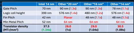
She then went on to make the claim that Intel 14nm has similar characteristics to others’ upcoming 10nm nodes (which have not yet been manufactured and reverse-engineered, so a table like the above cannot be produced.)
On the other hand, Intel was shipping FinFET devices all the way back on their 22nm node, and that is unquestionably a large lead over all competitors.
Speaking of 22nm nodes, Intel also seized the opportunity to announce a new power-optimized version of their 22nm process – dubbed 22FFL. The new process is designed for “low-power IoT and mobile products” and has a remarkable >100x leakage power reduction. Intel says the new process features simplified interconnects and design rules, better design automation tool support, and it is RF compatible. They claim the cost is competitive with other 28/22nm planar technologies. How does 22FFL shape up compared with the older 22nm and the new 14nm processes? The following table has the stats:
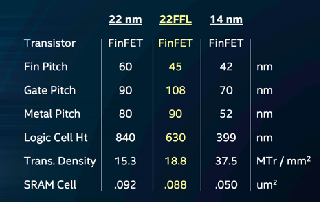
As you can see, 22FFL has a slightly better rating in the newly proposed MTr/mm2 metric than its older 22nm sibling despite a slightly looser gate and metal pitch. It also features both high-performance and low-leakage transistors on the same die, so designs can be power optimized by implementing high-performance transistors only where required and using low-leakage transistors for “always on” parts of the circuit.
Moving on to the future, Kaizad Mistry gave us a look at the details of Intel’s upcoming “10nm” offering (which, we were assured, will be significantly more advanced than competitive processes bearing the “10nm” moniker – a “full generation ahead” in fact). Intel 10nm will be produced with what the company claims will be the world’s first self-aligned quad patterning. (gulp). Note that no EUV sources will be harmed in these experiments.
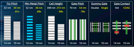
The following table shows 10nm feature sizes and hyper scaling enhancements compared with 14nm:
Mistry says this translates into a 2.7x logic transistor density improvement, or a whopping 100.8 MTr/mm2.
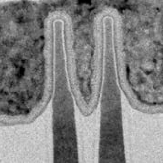
Whoa! Wanna see some nice photos comparing 22, 14, and 10nm FinFETs? Yeah, me too:
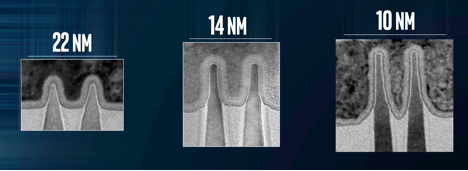
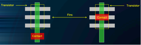
Mistry explains that 10nm fins are 25% taller and 25% closer spaced than 14nm. 3D transistors are getting MUCH more 3D. On the hyper scaling features, Mistry showed Intel’s new “contact over active gate (COAG) technology, which saves another 10% in area.
…as well as a “single dummy gate” technique, which saves another estimated 20% scaling benefit.
Finally, Intel explained the death of the famous “tick tock” technology release model. Historically, Intel has alternated releasing smaller-geometry processes every two years with enhancement releases on the in-between years. Moving forward, however, it will take about three years to complete a full process node. So, in the interim two year periods, we should see a “+” and a “++” process that optimize the previously released node. So, there will be 14, then 14+, then 14++, then 10, 10+, 10++, and so on. Each year’s release should bring additional optimizations, performance and power improvements, and cost reductions over the previous iteration of the same process.
There was considerably more ground covered in this breathtaking (and somewhat breathless) event, but we’ll save some of those revelations for another day.


