

Picture the huge datacenters run by Google and Facebook and their ilk. Imagine that, as big as they are, each of those datacenters serves only one company.
Now picture an Internet-of-Things (IoT) world where everything is connected, with data flying hither and yon, and with some non-trivial part of that data making its way to new datacenters built to handle the additional load. That could mean incredible distributed computing resources.
Even today, you may think of all the traffic that the internet sends to Google and Facebook – nothing to sneeze at, and yet it’s only part of the overall traffic they have to handle internally. For redundancy, performance, and scalability reasons, data is replicated and cached and optimized constantly, resulting in huge amounts of intra-farm traffic that never escapes the building.
This suggests that bandwidth will become a limitation as the traffic grows.
When wires and cables run out of steam, what do we turn to? Optical, of course. Minds are already imagining what might be necessary to implement fiber to a greater degree within these facilities. But to do that in a flexible way, you’d need to be able to route and switch the optical signals quickly and easily.
Optical switching is done today, according to a team at UC Berkeley’s Berkeley Sensor and Actuator Center, is really too slow for the job: switching takes on the order of milliseconds. It’s more useful for setting up more or less static routing – not for switching packets on the fly.
So this team, led by postdoc Tae Joon Seok, set out to combine silicon photonics and MEMS to build a crossbar switch that can switch in microseconds instead of milliseconds. And they didn’t want to build one of the little proof-of-concept switches that had been done already, but rather something on a more useful scale. So they built a 50×50 switch: 50 inputs, each of which can be routed to any of 50 outputs. It was presented at OFC 2015 (the Optical Fiber Communication Conference and Exposition).
First the photonics bits…
For those of you who, like me, spend little time with photonic concepts, I’ll refer you back to an earlier piece on silicon photonics basics. The photonics in this project are relatively simple; it’s the MEMS that adds some spice.
But there are a couple of photonics concepts I had to grapple with – things I conveniently omitted in the older article. One is the concept of “adiabatic.” And honestly, I’ve been a bit mystified about that all along – until recently learning that I was looking at the wrong “adiabatic.”
I vaguely remember learning the concept back as a college freshman gnashing my teeth over thermodynamics; I promptly forgot it after the final, and I haven’t seen it since. It has to do with processes that are heat-invariant. Not quite obvious how that affect photonics.
More recently, I stumbled across a note: quantum mechanics uses the word very differently. And this is the meaning that applies to photonics. It’s a relatively straightforward concept, conceptually (if anything thing can be considered conceptually straightforward with quantum…). Roughly stated, if you make a change gradually enough, the system can adapt.
I think of it as being like the boiling frog syndrome (trigger alert for those particularly attached to frogs). If you turn up the heat too fast, the frog notices and jumps out. If you do it slowly, then the frog’s eigenstate will change to reflect the final boiling Hamiltonian. Or something.
The obvious applications of this are in couplers, which typically have a gradual funnel shape, and with curves that can’t be too abrupt. If you change the dimensions gently enough, then everything can hum along in a stable state.
The second concept is that of optical signals that can cross through each other. If we were to build a wire-based cross-connect switch, we’d put the horizontal lines at one level and the vertical lines on another level; they would touch only if we enabled a connection from one level to the other. If you simply ran a grid of wires on one level – well, it would be a universal short, and not much would get done.
It would appear that this is not the case optically. Optical signals can intersect and cross each other and continue on their merry way without mutual interference. The details of how this works is something I’m frankly not comfortable with, so I’ll leave it as a further research project for the reader (or for me). Suffice it to say that the intersections are configured as what are referred to as “multi-mode interference,” or MMI*, crossings.
So the base level of this switch contains a grid of ridge waveguide, with MMI crossings at each intersection.
Then the MEMS bits…
The next question is, since the MMI crossings specifically keep the signal going straight, how do you make the signal turn a corner instead? If you want the signal on input waveguide 7, for example, to be routed onto output waveguide 10, you need something else. Those two waveguides cross each other but their signals will pass each other by with nary a wave hello.
This is where the MEMS comes in. And I’ll start by describing it in the simplest way I know how: it’s like a freeway flyover with hinged ramps.
After the team builds the initial photonic grid layer, they then build another layer above it, releasing underneath so that there’s space for the “ramps” to move. At each intersection, a switchable coupler is placed, as shown below. You’ll note that the underlying grid waveguide swerves so that the MMI crossings aren’t right underneath the MEMS element.
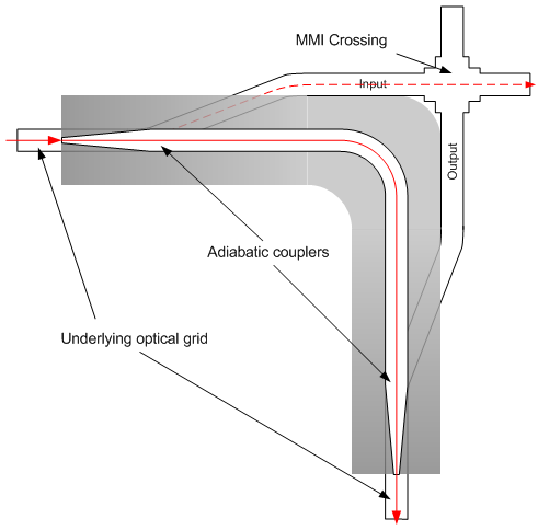
Figure 1. A single switch at an intersection. The shaded portion is the substrate supporting the upper curved waveguide; the ends can go up or down to break or make a connection between the horizontal and vertical waveguide. Highly stylized and simplified drawing; I’d call it an “artist’s conception,” except that I’m no artist.
The paper describing the project glosses over some of the MEMS details. The drawings make it seem like this entire upper structure – the couplings and the curve – rides up and down to make or break connections. I confirmed with Dr. Seok, and he said that, in fact, there’s a hinge at each ramp. So the curved portion remains stationary and elevated while the ends of the couplers rise and fall. The “hinging” consists of the ramp simply bending. The ramp is 50 µm long and dips by 1 µm, so the actual bend is gentle.
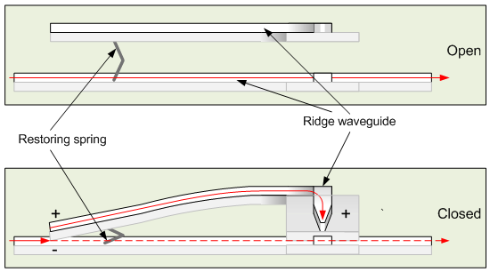
Figure 2. Side views of the switches, with both ends open (top) and closed (bottom). Again, highly simplified and stylized (with supports and stoppers not shown). Non-artist’s conception.
In the “open” position, the conceptual view above has all of the substrates and waveguides horizontal. The upper waveguide represents the switch and coupler; the lower waveguide is the grid, which would extend beyond the figure in both directions.
The lower figure shows the switch in the closed configuration, with both couplers actuated. The couplers are pulled down electrostatically (as indicated by the +/-); the couplers rise back up under the force of MEMS restoring springs.
You’ll also note that the coupler doesn’t quite touch the underlying waveguide in the closed position. This is intentional and carefully controlled: there are small stoppers built into the mechanism to ensure that the switches always land with a consistent gap. The gap when open is 1 µm; when closed, it’s 125 nm. At that gap, almost all of the light is captured by the flyover structure; the remaining signal (the dashed lines) is less than -20 dB.
There’s a switch like this at every intersection. Clearly the electrodes used for actuation must be addressable so that a controller can direct which switches to close. As far as I can tell, there’s no physical mechanism to prevent nonsense connections; seems like that would naturally fall to the controller to ensure.
The team claims this to be the first large-scale switch of its kind. With some luck, it may contribute to a new generation of high-bandwidth interconnections for massive computing centers.
*Yes, for you fellow MMI alumni, the acronym lives on in a number of contexts.
More info:
50×50 Digital Silicon Photonic Switches with MEMS-Actuated Adiabatic Couplers


Will this MEMS/photonics switch project help convert intra-data-center traffic to optical?