


They’d built up the sheep ranch over several decades. Starting small, they learned through experience how sheep thrive. They gradually diversified, experimenting with different breeds – this one for the smoothest wool, that one for higher quantities of milk to be used for feta and other cheeses – and, over time, they acquired solid confidence in their ability to manage the flocks.
But another similar animal started to gain popularity: goats – in particular for their milk, which they gave up in far greater quantities than sheep do. People often view sheep and goats as variations on a theme, so expanding the ranch to include goats seemed like a no-brainer.
Well, it turned out to be nothing like simply adding another breed of sheep. The goats behaved in ways that felt completely unpredictable as compared to sheep.
- While sheep were timid, even while relying on humans for protection, goats didn’t seem to care.
- While sheep stood around looking for a cue from someone as to where to go next, the goats just took off and explored everything, awaiting permission from no one.
- The sheep might dutifully eat the food in the trough; the goats would sample the food and then try eating the trough as well.
- Put down a shelter against the heat, and the sheep might sit in the shade; the goat was just as likely to climb up on top.
- Gaze at a sheep, and it would appear to be saying, “Uhhhhhh…. What?” Gaze at a goat, and it’s saying, “Did you like that last trick? Pretty cool, huh? I’m thinking of the next thing I’m going to do any second now. It’s gonna be even awesomer.”
This one “incremental” change ended up having far greater consequences than any of them expected.
EDA has been simulating semiconductors for decades now. Things have changed dramatically over that time, but, realistically, the biggest change has been one of scale: the amount of computation required today to simulate a production circuit would have been unfathomable back in the ‘70s when a modest little program called SPICE made its debut.
By solving moderately-sized sparse matrices, SPICE let engineers predict how various circuits might work before building them. And from here was launched a history of abstraction. Because, above a certain size, those matrices, however sparse, simply got too large to solve. We still haven’t been able to get around this for analog circuits, but digital circuits lend themselves well to abstraction.
So Boolean arithmetic let us solve complex circuits by reducing them to simple logic gates, each of which had been individually proven using SPICE. Now they could be combined – and their performance could be predicted – into simulatable circuits with thousands and millions and billions of gates.
In the meantime, we learned how to solve signal traces and power grids to analyze noise.
And, significantly, we learned how to predict how the materials used in the semiconductor process would behave. This involved understanding how etchants might impact resists and oxides and metals and silicon. It allowed for optical compensation once features dropped far below the wavelengths of the exposing light.
New materials and new processes would provide variations on what had come before, but, for the most part, the physics remained the same. And from the process layer level to the transistor level to the gate and block and full-chip level, EDA companies have incrementally built a vast trove of simulation knowledge and experience.
Looking forward, we’ve needed a bit of coloring help for multiple patterning, but we’ve managed to solve that one. Our experience will certainly remain relevant when/if EUV kicks in. Or if CEBL achieves mainstream status. Or when any of the new materials and techniques currently under study get incorporated into any of the reference processes.
Any, that is, except one: directed self-assembly, or DSA.
We’ve looked at the physics of DSA before (kind of), but we’ve never addressed the implications for simulation. I’m going to assume that “ab initio” or first-principles simulations are well established, but those serve well only during process development. They’re far too cumbersome for production use.
“How different could things be?” you wonder. While all the DSA-related papers at SPIE litho are full of hints that this is a different world, one in particular caught my eye this year: a paper* from a team from Kyoto University and Toshiba focusing on design-for-manufacturing (DfM) for DSA.
My first thought was that DSA has come a long way – in a couple of years it’s moved from “Here’s a weird new idea that we might be able to make use of” to “How can we create layouts that will give reliably high manufacturing yields?” That’s pretty incredible.
But what really caught my eye were the images in this work. We know in general that these DSA block co-polymers (BCPs) like to separate out and create nice neat rows of straight lines when confined or “directed” by neighboring or underlying structures. But if you think about it in more detail, what we’re talking about here is a complex liquid. It’s like oil and vinegar, only with the oil and vinegar molecules tied to each other and each side of that bond trying to distance itself from the other.
This brings us face to face with the physical processes that form droplets and menisci: the forces that govern how a blob of oil in vinegar will behave. All of which have little in common with the physics of optical lithography and traditional etching.
This particular paper focused on the formation of contact holes, and the images you’ll see are from their paper and their low-level simulations (used with permission). Let’s start with a simple example.
The way DSA helps to create a small contact is related to how we get thin parallel lines – except that now things are circular instead of linear. You first create a (relatively) large hole in a hardmask material, which acts as the guide.
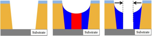
Figure 1. Basic hole creation process. (Image courtesy SPIE and authors*)
This hole gets filled with the BCP, which then self-separates (referred to as “phase separation”), and the expectation is that you now have an inside cylinder surrounded by an outside shell – kind of like a bagel dog. (I started to say “corn dog,” but that’s not really right – the ends of the central core should be exposed.)
Now, selectively etch away the part in the middle and you end up with a hole through which you can etch down into the substrate. The idea is that this hole – the inside cylinder – is much smaller than what you could easily print using conventional lithography.
Let’s start by looking at this from the top. The following image shows a simulation of the process we just described as viewed from above.

Figure 2. Separation for single contact hold. (Image courtesy SPIE and authors*)
The red and blue indicate the two self-repelling components of the BCP (I’m not going to worry about the specifics of the chemistry because it doesn’t matter for our purposes). In this case, the blue has migrated outward and the red has remained in the middle. From here, the red material is selectively etched away, providing a nice small hole.
We can reinforce the periodic nature of this by starting with a bigger guide hole. The example we just saw is clearly sized to where you get one ring of blue around a red center. If you make things wider, then, for a while, the center hole gets bigger. But at some point, you cross the period of the material, and now you get repeats that show up as concentric rings. Keep getting bigger, and you’ll get more concentric rings.
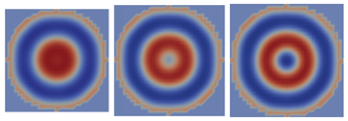
Figure 3. Effects of larger guide hole. (Images courtesy SPIE and authors*)
This is all well and good, but it’s only the top view. We’re used to assuming that whatever we see on top can be projected – or “transferred” – down through the material. Alas, here’s where our experience starts to fail us. Because this separation happens not just in 2D, looking at the top, but in 3D. These are essentially liquids (at least while separating), so the convenient expectations of the past won’t hold.
In fact, the whole reason that the research team investigated this scenario was because, when removing the middle core, it didn’t seem to be clearing all the way down to the substrate, and this was causing a significant yield issue. And, critically, this is not something you can see by inspecting a wafer.
So let’s look at these simulations from the side. The first one shows that the central core isn’t, in fact, reaching all the way to the bottom. As the BCP separates, some of the blue takes up residence at the bottom. When the red is etched away, a bit of blue remains and prevents the substrate from being etched.
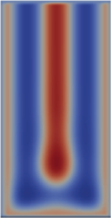
Figure 4. Side view of Figure 2. (Image courtesy SPIE and authors*)
Now… as an aside, it turns out that a solution to this problem is to “brush” the bottom with one of the copolymers to bias which one prefers to “stick” to be substrate – forcing the red material all the way down. In theory, problem solved.
But my interest here is less on the specific DfM aspect and more on the surprising shapes – or “morphologies” – that result as you give the BCP more room to spread its wings. So let’s look at the other three wider holes we saw in Figure 3.
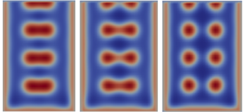
Figure 5. Side views of the holes in Figure 3. (Images courtesy SPIE and authors*)
Bet that wasn’t what you were expecting. From the top, the center hole was simply getting wider until it finally split into a new ring. But lurking underneath, hidden from our innocent, prying eyes, all sorts of mayhem was underway. First the column segmented into disks. Then the disks started clearing out in the middle to form tori (i.e., mini-donuts… No, Homer – don’t even think about it).
And all hidden from inspecting eyes.
Another experiment involved not expanding the guiding hole uniformly, but stretching it in one dimension only. As you can see below, the periodicity in this case provides multiple contacts closely spaced. But again, under the surface, interesting morphologies are at play.
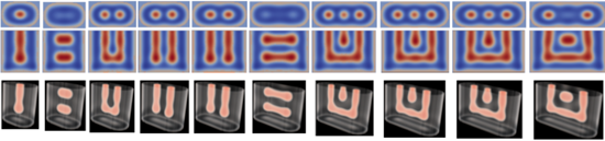
Figure 6. Stretching the guide hole in one direction only.
(Image courtesy of SPIE and authors*)
Fixing defectivity is a high priority for DSA. So somehow, some way, tools will be needed to evaluate real-world layouts to evaluate the 3D shapes that are likely to result. This is not an incremental addition to current simulations; this is a whole new animal.
EDA, you’ve just received some goats to add to your flock of sheep.
Images used by permission from SPIE and the authors. Ken Fukawatase; Kenji Yoshimoto; Masahiro Ohshima; Yoshihiro Naka; Shimon Maeda, et al.: “DFM for defect-free DSA hole shrink process”, Proc. SPIE 9049, Alternative Lithographic Technologies VI, 90491K (March 27, 2014)


Are you seeing production EDA tools that take into account the peculiarities of the block copolymers used in DSA?
Bryon
Was your title a ruse to get more readers or is your average reader supposed to already know what “DSA” is? I hate having to skip paragraphs to find out what an article is about! 🙁
You hit on a common tension that we have to navigate. I could have put “Directed Self-Assembly” in the title, but likely, if you didn’t know what DSA is, then having it spelled out wouldn’t have helped because it’s a specialized technology. I went on the assumption that semi folks would understand it, and that EDA folks that might not know it would be pulled in by the “EDA” portion (where I’m also assuming knowledge of what “EDA” stands for).
It’s tough to know which TLAs (three-letter acronyms) to assume people know. And I know that I sometimes fall on the “assuming too much” side of things just because I swim in this stuff all the time – not all readers do. Add to that my occasional desire to do a whimsical start, and yeah, the hook (or “lede”) gets pushed down.
So your point is well-taken. Not sure there’s an easy answer for this specific title, but in general… understood.
Hi Mr. Moyer,
thank you for the interesting article.
I know about a few small companies working with DSA here in Japan, but so far their results is limited to very simple patterns with very large variations.
I wounder how it may be possible to build 3D FinFets needed in ICs using DSA .. Is it even conceivable or has anyone tried to do that so far?
From what I’ve seen, one of the applications of the “line” flavor (as opposed to “hole” flavor, which we looked at here) is to define the fins. In other words, a long line would be built (or, realistically, a set of lines for multiple fins) and then cuts made to define the extent of the fins. I’d have to review the literature to see what, if any, results have come from this. No doubt it’s still early days.