

It’s said that the best way to learn something really well is to teach it to someone else. A close corollary to that would be simply to write about it. Which we in the press have to do all the time. So what happens when we don’t quite understand what we’re writing about?
Oh, wait, I’m not sure if I was supposed to say that. You know, inner circle of writers, never admit we know less than we do, etc. Well, I’ve said it; the damage is done. If you never hear from me again, just assume that my colleagues weren’t particularly pleased with me outing us.
So there are five ways of dealing with our knowledge gaps:
- The easiest is to use 3rd person: “So and so claims that…” This way you absolve yourself of any specific knowledge, and you just pass on what someone else said. This is the most common approach by far.
- Ask lots of questions of the source to fill the gaps. This requires a patient source who will tolerate your sorry-assed questions that will typically arrive at the last minute.
- Just pretend you know what you’re talking about and hope that no one knowledgeable enough will read you or call you on it.
- Pick a different topic. (Who knows how often this is done…)
- Fess up. (Not likely.)
I had to decide which of these routes to take for my topic today. When I first saw it and studied it, I decided, “Yup, I’ve got this.” And I mentally set it aside until time to write the piece. And then I started writing. And the questions started coming. And they ultimately boiled down to one fundamental question. Which is… well, let’s wait on that. All in good time.
Let’s start with a problem that needs solving. And that relates to the variability of MEMS devices as actually built. Semiconductor ICs have had to deal with variability on a huge scale at the most aggressive process nodes, spurring major efforts in changing how designs are done and guardbanded. But with ICs, we’re correlating geometry to electrical properties, and chip volumes are huge, so we can go in and make huge EDA research investments to solve this problem.
MEMS dimensions, by contrast, are enormous when viewed in the context of a 20-nm process – no one is applying variation techniques here. And, with MEMS, geometric variation leads to mechanical variation, which leads to electrical variation – there’s that additional mechanical step in the middle. Combine this with MEMS being something of a boutique industry historically – which is changing – and you end up not having the analytical tools to figure out exactly how ideal layouts will turn out on any given die (although this is getting better).
Even if you know the range of results that you might get more accurately, you’re still left with calibrating individual devices. And the problem is that the various schemes for characterizing and calibrating against deviations from the ideal are themselves very inaccurate. And errors can propagate and multiply to yield uncertainty that swamps out what you might be trying to achieve.
An example given at the recent MEMS Testing and Reliability conference is that of trying to determine the force deflecting a cantilever. The force is the product of the cantilever stiffness and the actual displacement. If the stiffness is measured to be 4.73 N/m ±10% and the displacement is measured to be 9.62 nm ±10%, then the force lies somewhere between 36.7 and 55.1 nN – a huge range.
A team at Purdue University has tackled this problem with a different approach: rather than trying to eliminate all of the inaccuracies inherent in measurement processes, can we measure something directly on the die that will act as a proxy and bypass the inaccuracies?
This requires going to some first principles and involves a lot of unknown variables. The team has focused on the comb drive structure in their work. The whole principle of a comb drive is that interleaved fingers overlap by some amount, and the capacitance between the fingers is determined by the amount of overlap. The coefficient of proportionality (in the regime where it’s linear) is the comb drive constant ?.
Now, based on first principles, the comb drive constant is given in the paper as:
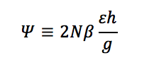
where:
– N is the number of comb fingers (known)
– ? is the fringing field correction factor (unknown)
– ? is the permittivity (unknown)
– h is the layer thickness (unknown)
– g is the effective gap between the fingers (unknown)
In other words, most everything needed to determine ? is unknown. There may be design-based numbers that could be used, but those are targets, not actuals; here we need true as-built data that we don’t have.
The Purdue approach is to build a stationary feature in the middle of the comb drive, but have it offset so that it’s closer to one side than the other. This creates two unequal gaps on either side of this “anchor.”
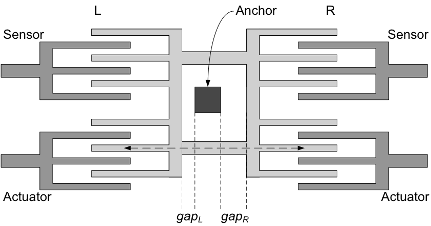
The idea is that you can actuate the comb and move it left until it bumps the anchor and then right until it bumps the anchor. Even though the structure is designed with a specific spacing around the anchor, that’s not necessarily what prints; by sliding the comb, you figure out what the true distance is; they refer to it as ?gap. In other words, to a first approximation,
gapL = gapL,layout + ?gap
gapR = gapR,layout + ?gap
This isn’t quite correct, since there’s no guaranteeing that the left deviation is the same as the right one; the right one can be modified by a factor (1+?) to account for this, and they discuss possible ways to characterize ?, but we’ll proceed without that. Also, because the anchor is intentionally off-center, the right gap is some multiple n of the left gap, so that second relationship becomes:
gapR = n gapL,layout + ?gap
Sliding the comb to the left and right results in a change in capacitance ?CL and ?CR, respectively; this results in a comb drive constant for the left and right ?L and ?R. If we knew the actual gap, then we’d know the constant, but the whole problem is that we don’t know the actual gap, so we can’t figure out the constant.
However, by ratioing the two measured changes in capacitance, we end up dividing out the drive constants:
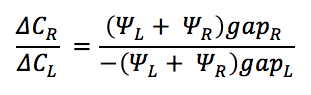
and we can put the whole thing in terms of the left gap:
![]()
From this we can solve for ?gap:
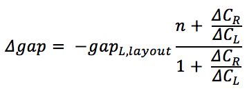
In other words, we can determine the gap deviation from layout using only layout information and the measured changes in capacitance. Capacitance can be measured very accurately, and the effects of other parasitics that may change from time to time have also been cancelled out, making this a repeatable measurement.
Ordinarily, this deviation would be measured optically or by SEM or some other such approach. But non-idealities like feature roughness and non-vertical walls add significant uncertainty that can be improved using this electrical measurement.
Now, if you’re me, you slog through this, following all the steps (many of which I have omitted above), and you come out the end feeling triumphant: “Yeah, I get it!”
Then, as the euphoria wears off, it suddenly occurs to you: “Um… OK, we found the gap deviation. What does that tell us?” And the furrowed brow returns.
Well, now we know the actual gap that was traversed during the test for the left and right, so now we can determine the comb drive constants. And there are several other characteristics that evolve from that:
- Knowing the drive constant, we can calculate the displacement for any arbitrary change in capacitance.
- The force applied to the comb can be determined by the drive constant, change in capacitance, displacement, and voltage used to actuate the comb.
- The force and displacement give us the stiffness.
Likewise, we can determine the mass, damping, and Q of the system.
So that’s all good. But there still remains one high-level question. It’s not really addressed in the paper and presentation that describe the Purdue work. You don’t really think of it at first because the descriptions start by motivating the lack of accuracy of various measurement techniques, which you buy off on, and then you immediately get sucked into the detail. It’s only when pulling back out and digesting for a few moments that you suddenly realize: “I’m not really sure specifically why we’re doing all of this.” Yes, it gives us some data more accurately than measuring it would do, but… so what?
Murphy has assured that such questions will arise within days of a deadline. And the person with the answers will be busy or away or who knows what. And you’re left to answer it for yourself.
There were four possibilities that occurred to me:
- By measuring the gap deviation, we can tell something about the process and extrapolate that to the whole die. Well, maybe, but not likely. The very fact that a ? element has been considered in the work suggests that the deviation on the left and right sides of the anchor may be different. If that’s the case for features that are so close, then you pretty much can’t count on knowing anything about any other part of the die from this one measurement.
- What we learn about the comb drive characteristics gives us fundamental information that can be applied to a host of other structures on the die. Still seems unlikely since the gap information is localized and, as far as I’ve seen, that gap hasn’t been used to motivate any more fundamental parameter.
- What we learn about the comb drive can be extrapolated to other comb drives on the die. Again, because the gap information is local, this would seem not to be the case.
- What we learn about the comb drive tells us a lot about that specific comb drive. This seems the most likely result to me.
I posed this question, and, as of this writing, I haven’t (yet) received an answer. (If I receive one at the last minute, I’ll add it as a note below… if I receive it after publication, I’ll blog the response.)
Assuming I’m right, what that means is that each structure about which we want accurate information must be given its own calibration structure. The gap concept works for comb drives; some other method must be used for other elements. Simple MEMS dice have few structures; integration may change that. So proliferation of test structures must be balanced against their die-size implications. It would appear that the researchers have looked beyond the comb drive to generalize it more broadly, since they’ve given the whole concept the moniker of “electro-micro-metrology,” or EMM.
So, as it turns out, I have actually opted for option 5 above: I’m confessing my ignorance, while taking you as far as my brain can take it and leaving the rest of the journey to you. Feel free to add your own thoughts below.
More info:


How much leverage do you think you could get out of this MEMS self-calibration technique? Just data about the one structure? Or more?