

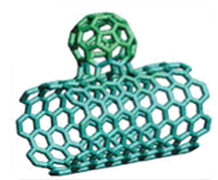
flexible material that can be made to conform to pretty much any shape. While this stretchability is a function of the substrate, its conductivity comes from a marriage between a carbon nanotube (CNT) and a Buckyball into a “nanobud.”
(Image courtesy Canatu)
The company is Canatu, and they coat flexible plastic substrates via a room-temperature printing process with this CNTish material; that layer can then be patterned according to the application. In their manufacturing process, the nanobuds self-assemble on the CNTs.
The nanobuds appear to help with the conductance. Yes, CNTs can allow ballistic charge transport, but, so far, we can’t make inches-long CNTs and line them all up next to each other. So the inks used to print the CNT materials contain short CNT strands (20 µm, which Canatu says is actually long compared to typical CNT inks). The idea is that, as long as these strands touch each other, electrons can travel ballistically as far as they can, and then they hop onto another CNT and continue their journey.
Canatu believes that the nanobuds assist in assuring good contact between adjacent CNTs, improving electron flow. Good density and good contact would be particularly important for a material that is going to stretch (which would increase the average separation between strands).
The following is how Canatu’s layers would be integrated into a touch application (like the virtual clipboard shown).*

(Image courtesy Canatu)
There’s a key distinction between some other touch materials and Canatu’s approach: in some other cases, you “pattern” with lines (perhaps fine metal lines), and the lines themselves are the conductors. It can be the opposite here: the coating does the conducting, and lines can be patterned to separate the coating into regions that can then be used to figure out where touch is occurring.
So, for example, a slider may be patterned as chevrons; each chevron slice registers as a finger runs along it. A two-dimensional implementation would use two layers: one striped in the X direction, the other in the Y direction.
But such flat implementations aren’t the only ones possible. Canatu has three versions of their material:
- Hi-Contrast: this is intended for flat applications like your basic touchscreen; they claim zero haze and zero reflectance. This is an existing product.
- Flex: this can be applied on 2.5D surfaces (that is, you can bend either in the X or Y direction, but not both). Once applied, it can be flexed in any direction. It also shares the clear characteristics of the Hi-Contrast product. Also an existing product.
- In-Mold: this has been newly announced, and it’s a completely stretchable (up to 120%), moldable, 3D-flexible film that can be applied to most any kind of terrain. The ink is applied on the film while flat, and then the film can be fitted to its surface. It’s a bit darker than the other two because it has a different substrate, but if the surface onto which it’s applied isn’t a screen, then that probably doesn’t matter.

(Image courtesy Canatu)
Electrically, this touch material looks like ITO, so standard ITO controllers can be used when assembling a system.
As far as cost goes, the flat hi-contrast material is priced just under high-quality ITO. For 2.5D and 3D, there’s no ITO competition, so there’s less to keep a cap on the cost… But Canatu says that the film isn’t the cost limiter in such systems.
You can find out more about their new In-Mold version in their latest announcement.
*“OCA” is “optically-clear adhesive.”


