

Any new foundry would want to grow up to be a megalith like TSMC, right? Isn’t that how you prove you’ve “made it”? Well, not if you’re Novati. They’re a different sort of foundry, one you don’t hear about so often over the noise of the Big Guys.
Here’s the thing: when you’re in the foundry mainstream, you do one thing: you chase Moore’s Law and try to keep it going. You figure out what the masses want, and you trim everything extraneous away so that you can sate the masses in enormous volumes at competitive costs.
But what if you’re in the market for something that can’t be made using the techniques that suit the masses? That’s where smaller… ok, I’m going to use the dreaded word (investors: please cover your ears): niche players can find plenty of business, even if, by so doing, they can maybe achieve only kilolithic or decalithic status.
I met with them at Sensors Expo. Sensors are a typical opportunity for a more flexible fab, since they may use unusual techniques and materials, and each one may be slightly different, making it hard to put everyone onto one high-volume recipe.
Novati does CMOS and MEMS (particularly silicon microfluidics) – jointly and severally. When jointly, with both on the same wafer, they typically do MEMS-last, placing the MEMS elements above the CMOS circuitry. They can do this either by growing more silicon epitaxially over the CMOS or by stacking a separate wafer.
They also work on silicon photonics projects and 2.5D (silicon interposer) and 3D integration.
Most of what they do leverages a common set of equipment (largely for 200-mm wafers, with some 300-mm ones), but where the diversity really comes in is with materials. They can work with 60 different elements – far more than would be found in your average foundry.
Most foundries want to keep the number of elements they allow through the door to the absolute minimum. A new material, if not handled carefully, brings with it the risk of unexpected contamination with potentially calamitous results – something that’s just not worth messing with if you’re spinning oodles of wafers an hour.
But smaller guys need to be more flexible, and a willingness to work with more materials can be a boon to developers trying new ideas. Gold is the one element that Novati is particularly careful with: They segregate that in a separate room. For all the others, they study each one under consideration and develop specific protocols to ensure that the material goes only where they want it to. Which may be limited to some nanolayer a few atoms thick laid down by atomic layer deposition (ALD) on a wafer.
Once a project gets to production volumes, they can handle it to an extent, but they may also hand off to a partner that can handle higher volumes. Of course, if the volume production involves odd materials, then they’ll need to work with someone willing to handle that material.
As with any business, there’s always opportunity on the fringes of the mainstream. In this case, they’re entertaining many of those opportunities; they’re just being careful not to step on Moore’s toes.
You can find out more on their site.
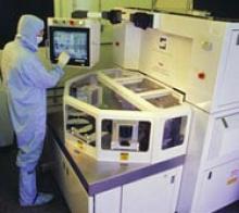
(Image courtesy Novati)


