editor's blog
Subscribe Now

TSVs: Like Vias, Only 1000X Deeper

We recently looked at Applied Materials’ solution to the challenges of lining small vias: using cobalt. But those are through-dielectric vias. What about through-silicon vias (TSVs)? After all, they can be a thousand times deeper than a standard via, so if a standard via is hard to cover, imagine how hard it must be for a TSV.

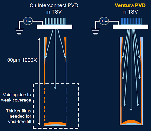
Of course, we’re talking a wider via, but AMAT says that standard physical vapor deposition (PVD) tools do an inadequate job of coating the TSVs when applying the barrier, for lots of the same reasons we discussed in the cobalt story.

Their solution to the TSV issue isn’t quite as radical as a new metal; it involves tightening up the angle of dispersion for the metals, providing better coverage. With better coverage, the barrier can also be made thinner, saving cost. A thinner layer is faster to deposit, improving throughput (and reducing cost).

Figure.png


(Image courtesy Applied Materials)

In addition, they’ve built a production-worthy chamber for use with titanium rather than the more typical “proven” tantalum. Titanium apparently being cheaper than tantalum. Both can be integrated with the copper seed.

You can read more about their Ventura PVD in their announcement.

Leave a Reply

featured blogs
Apr 25, 2024
Structures in Allegro X layout editors let you create reusable building blocks for your PCBs, saving you time and ensuring consistency. What are Structures? Structures are pre-defined groups of design objects, such as vias, connecting lines (clines), and shapes. You can combi...
Apr 25, 2024
See how the UCIe protocol creates multi-die chips by connecting chiplets from different vendors and nodes, and learn about the role of IP and specifications.The post Want to Mix and Match Dies in a Single Package? UCIe Can Get You There appeared first on Chip Design....
Apr 18, 2024
Are you ready for a revolution in robotic technology (as opposed to a robotic revolution, of course)?...

featured video

MaxLinear Integrates Analog & Digital Design in One Chip with Cadence 3D Solvers

Sponsored by Cadence Design Systems

MaxLinear has the unique capability of integrating analog and digital design on the same chip. Because of this, the team developed some interesting technology in the communication space. In the optical infrastructure domain, they created the first fully integrated 5nm CMOS PAM4 DSP. All their products solve critical communication and high-frequency analysis challenges.

Learn more about how MaxLinear is using Cadence’s Clarity 3D Solver and EMX Planar 3D Solver in their design process.

featured paper

Designing Robust 5G Power Amplifiers for the Real World

Sponsored by Keysight

Simulating 5G power amplifier (PA) designs at the component and system levels with authentic modulation and high-fidelity behavioral models increases predictability, lowers risk, and shrinks schedules. Simulation software enables multi-technology layout and multi-domain analysis, evaluating the impacts of 5G PA design choices while delivering accurate results in a single virtual workspace. This application note delves into how authentic modulation enhances predictability and performance in 5G millimeter-wave systems.

Download now to revolutionize your design process.

featured chalk talk

Gas Monitoring and Metering with Sensirion SFC6000/SFM6000 Solutions
Sponsored by Mouser Electronics and Sensirion
In this episode of Chalk Talk, Amelia Dalton and Negar Rafiee Dolatabadi from Sensirion explore the benefits of Sensirion’s SFM6000 Flow Meter and SFC Flow Controller. They examine how these solutions can be used in a variety of applications and how you can get started using these technologies for your next design.
Jan 17, 2024
14,168 views