With all the delicacy involved in the advanced lithography techniques we use for patterning exquisitely small features onto wafers, occasionally we come back to a brute-force approach: nanoimprint lithography (NIL). Instead of painstakingly exposing patterns onto a photoresist, we simply press a patterned die (PS this is the kind of die whose plural is “dies,” not the singulated silicon bits whose plural is “dice”) into a bed of moosh to create a pattern as if making an old-school vinyl record. Harden the material, and we’re good.
While already used for hard drives, we’ve also seen it combined with DSA for even more aggressive hard drives. But that’s all still research stuff.
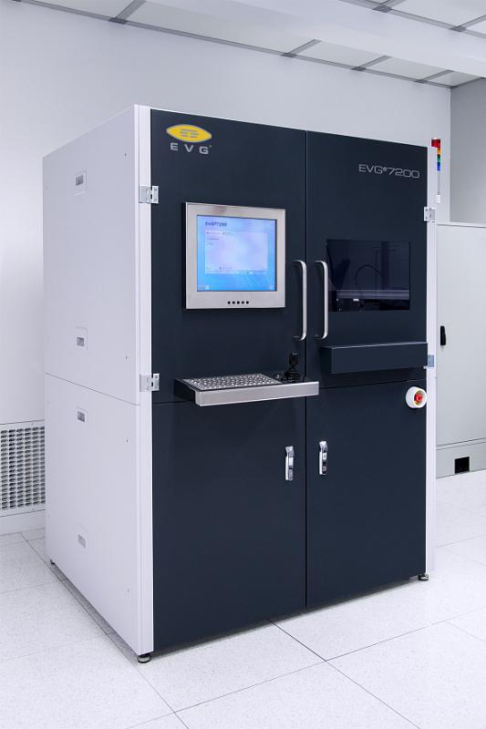 EVG recently announced a high-volume production SmartNIL process. It’s a UV-cured approach, although any of you wondering why they get to use UV while EUV is stuck at the starting gate have no reason to be jealous. Unlike EUV, you don’t need a carefully collimated beam of UV. You can just bathe your wafer in incoherent swaths of UV light.
The obvious question then might be, why can’t I use this? And the answer is, maybe you can! From a target-technology standpoint, your odds are good. (From a number-of-designers standpoint, not so much). It’s easier to answer the question, “What can’t this be used for?” than, “What can it be used for?”
The answer to the easier question is, “Transistors.” There are two issues with NIL for advanced transistors: feature size and defectivity.
- Yes, according to EVG’s Gerald Kreindl, advanced research work in John Rogers’ group at Illinois has actually replicated a carbon nanotube (CNT) using imprint. (Which is interesting since a CNT is a 3D feature…) The point being, there’s not a fundamental limit to feature size. (OK, there is, but I don’t think anyone is going to try to replicate a quark using NIL) Realistically speaking, SmartNIL is for features in the 20-100-nm (or bigger) range (more like 40 and up in high volume). That would leave out fins, for example.
- The other issue is defectivity: a slight glitch in a microfluidics channel isn’t going to cause any pain. That same glitch in a transistor may send valuable electrons in the wrong direction.
So if transistors are out, what does that leave? Lots: Optics, photonics, LEDs, bioelectronics…
You can find out more in their announcement.