

Intel really has two businesses: selling microprocessors and manufacturing silicon. The two are related in obvious ways, but they’re not actually the same thing. Most of Intel’s competitors, including AMD, Texas Instruments, MIPS, IBM, nVidia, ARM, and others create microprocessors but they don’t manufacture them. Meanwhile, semiconductor foundries like TSMC, Global Foundries, SMC and others manufacture silicon but don’t (usually) design chips. Intel is one of the few companies that do both.
That’s important because it means Intel has to grow in two dimensions at once. It’s not enough for the company to simply roll out a new CPU every few months. They’ve also got to coordinate those CPU design cycles with their manufacturing technology cycles. One side of the business feeds the other, and the combination of the two is what gives Intel its unusual punch in this industry.
To some industry observers—and I include myself here—Intel’s real strength is its manufacturing prowess, not its microprocessor chips. Those guys can build anything. The company’s first-rate semiconductor technology makes up for some inherent defects in its x86 product line. Not that Intel’s CPU designers aren’t also top-notch; it’s just that the x86 architecture doesn’t always compliment today’s market requirements. Consumer and communications products generally aren’t a good fit for Atom or Xeon or Itanium, but darned if Intel doesn’t do a good job of shoehorning them in anyway. As an Air Force pilot once observed, “with a big enough engine, even a brick can fly.” Intel’s manufacturing technology is that engine.
Engines sometimes need a rebuild, or even a complete overhaul, and that’s what Intel announced a few days ago. The company pulled the wraps off its next-generation semiconductor fabrication technology, designed to work at 22nm geometry. (Intel’s current state-of-the-art chips are made in 32nm silicon.) Due to roll out in new CPU chips in less than a year, the 22nm process is pretty impressive. It’s not just a shrink from current geometry, it’s structurally different. Intel calls it “3D” and “tri-gate,” two terms that have confused some members of the general press, the poor dears.
In practice, Intel’s new 22nm silicon will help the company maintain a lead over its closest rival AMD and help close the gap between its own x86 chips and those based on ARM or MIPS architectures. It won’t suddenly leapfrog Intel into the forefront of low-power, mobile applications. But it will give the company a big lever to use to pry open some design wins.
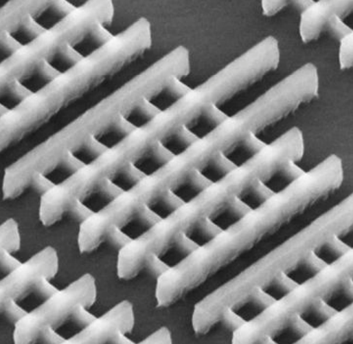
The “3D” description of the new 22nm process is partially true, but it’s not as exciting as it might sound. Silicon chips have always been three-dimensional, with multiple layers of silicon, oxides, and metals stacked one atop the other like layers on a wedding cake. We’ve all seen the blurry electron microscope images that show gates and interconnect arranged in tidy rows. But for the most part, those features are neat, rectangular brick shapes. Like microscopic 2×4’s, semiconductor features look like lumber arranged in neat rows. Intel’s new 22nm process tweaks that a little bit by overlapping some features, so that part of the gate crosses up and over the top of a narrow silicon “fin” of the substrate.
Normally these features lie on top of each other, with one side of the gate (the bottom) contacting one side (the top) of the silicon. Charging the gate alters the conductive properties of the silicon, allowing current to pass underneath. By building up this little fin and draping the gate over it, you now have three points of contact (hence, “tri-gate”), on the top and both sides. This increases the surface area of the contact patch without increasing the overall size of the transistor itself. This does all sorts of good things, like increase power efficiency and reduce leakage current. It’s faster, too, but that’s normal for any process shrink.
Is Intel’s new 22nm process technology impressive? You betcha. Is it a game-changer? Nope. The company is almost always at or near the leading edge of process technology, and this new generation is no different. Not to belittle Intel’s developments—this stuff is truly mind-blowing magic—but we’ve grown accustomed to semiconductor companies improving their process technology every few years. It seems normal. Just like the public eventually got bored with space shuttle launches, the semiconductor industry tends to greet multibillion dollar leaps in silicon technology with a collective “Ho hum.”
Intel plans to roll out its shiny new silicon first with Ivy Bridge, the codename for a Core processor descended from the current Sandy Bridge part. That’s probably less than a year away now, so Intel is well along the path to productizing its new technology. The first plant to use it will be in Oregon, with Arizona and Israel getting the upgrade later. Eventually, this process will get used for all of Intel’s processors, from Atom at the low end to Itanium at the high end. It also marks the end of Intel’s “planar,” or normal, fabrication technology. Every process generation from here on out will use the tri-gate arrangement rather than the flatter organization we’re used to.
It’s worth pointing out that Intel isn’t alone in this race. IBM, Global Foundries, and TSMC are all working on similar technologies that will bring most or all of the same benefits. Intel just got there first. The Santa Clara company believes it has a three-year lead over its rivals; we’ll have to wait until 2015 to see for sure.
It’s amazing, really. Semiconductor transistors are one of the most exotic inventions in human history, yet they’re more plentiful than grains of rice. Tens of millions of transistors fit on a single microprocessor chip, and billions on a wafer. Chip-making plants are staggeringly expensive (figure $5 billion or so), the raw materials that go into them are cheap, and the products they create are ubiquitous. Semiconductor clean rooms are a thousand times more sterile than a hospital operating room, and the workers are suited up like astronauts, not to protect themselves but to avoid contaminating the chips. Yet the price of a single transistor is so small as to be incalculable. They’re essentially free. It’s organizing them, designing them, and programming them that adds value and creates a whole industry. Good work, guys.
Image: Intel Corporation


