fresh bytes
Subscribe Now

How to clear a path through 60 feet of snow

tateyama.jpg

Mt. Tateyama rises 9,892 feet in Japan’s Hida Mountains and is considered one of the country’s Three Holy Mountains. It also may be one of the snowiest mountains in Japan, and perhaps one of the snowiest places on planet Earth.

The Hida Mountains are part of the Japanese Alps and meteorologists suspect that parts of the range receive as much as 1,500 inches of snow a year, or 125 feet. Piled continuously, that would be snow nearly half as high as the Statue of Liberty.

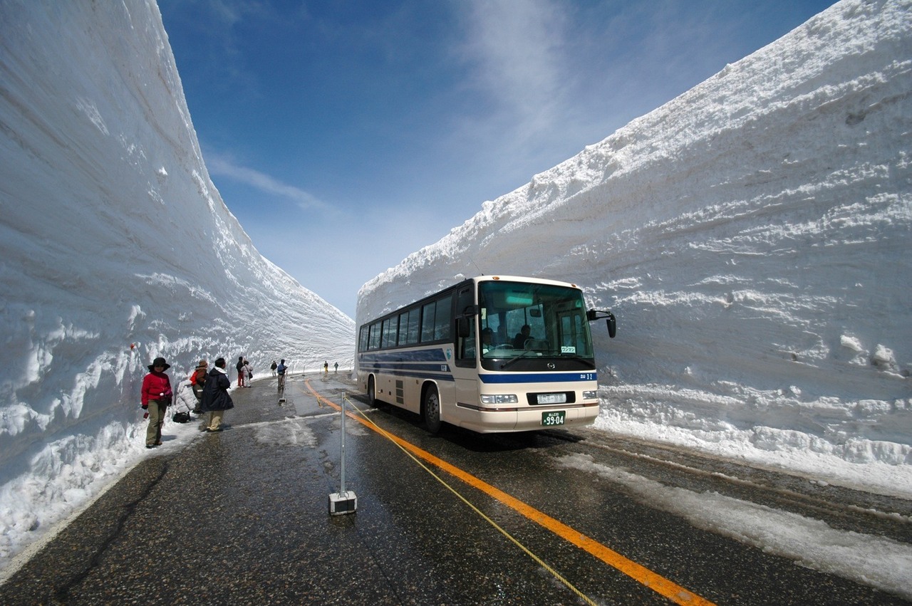
Amazingly, there is a highway that runs through a part of this epic snow country. Route 6 begins in the 420,000-person coastal city of Toyama, approaches the western flank of Mt. Tateyama, then disappears into a tunnel. The route eventually emerges on the other side of the Hida Mountains, in Nagano Prefecture, where the 1998 Winter Olympics were held. But just before the road enters the tunnel—and just after it passes the remote and The Shining-esque Tateyama Kokusai Hotel—it runs for about a quarter-mile along the base of a broad ridgeline. In Japan this particular stretch of highway is known as yuki-no-otani, or Snow Canyon.

The height of the canyon’s snow walls can reach a staggering 66 feet. via Atlas Obscura

Continue reading

Leave a Reply

featured blogs
Apr 25, 2024
Structures in Allegro X layout editors let you create reusable building blocks for your PCBs, saving you time and ensuring consistency. What are Structures? Structures are pre-defined groups of design objects, such as vias, connecting lines (clines), and shapes. You can combi...
Apr 25, 2024
See how the UCIe protocol creates multi-die chips by connecting chiplets from different vendors and nodes, and learn about the role of IP and specifications.The post Want to Mix and Match Dies in a Single Package? UCIe Can Get You There appeared first on Chip Design....
Apr 18, 2024
Are you ready for a revolution in robotic technology (as opposed to a robotic revolution, of course)?...

featured video

MaxLinear Integrates Analog & Digital Design in One Chip with Cadence 3D Solvers

Sponsored by Cadence Design Systems

MaxLinear has the unique capability of integrating analog and digital design on the same chip. Because of this, the team developed some interesting technology in the communication space. In the optical infrastructure domain, they created the first fully integrated 5nm CMOS PAM4 DSP. All their products solve critical communication and high-frequency analysis challenges.

Learn more about how MaxLinear is using Cadence’s Clarity 3D Solver and EMX Planar 3D Solver in their design process.

featured paper

Designing Robust 5G Power Amplifiers for the Real World

Sponsored by Keysight

Simulating 5G power amplifier (PA) designs at the component and system levels with authentic modulation and high-fidelity behavioral models increases predictability, lowers risk, and shrinks schedules. Simulation software enables multi-technology layout and multi-domain analysis, evaluating the impacts of 5G PA design choices while delivering accurate results in a single virtual workspace. This application note delves into how authentic modulation enhances predictability and performance in 5G millimeter-wave systems.

Download now to revolutionize your design process.

featured chalk talk

FlyOver® Technology: Twinax FlyOver® System for Next Gen Speeds -- Samtec and Mouser
Sponsored by Mouser Electronics and Samtec
In this episode of Chalk Talk, Amelia Dalton and Matthew Burns from Samtec investigate the challenges of routing high speed data over lossy PCBs. They also discuss the benefits that Samtec’s Flyover® cable assembly systems bring to data center and embedded designs and how Samtec is furthering innovation with their high speed interconnect solutions. 
Apr 15, 2024
1,431 views