


At present, we have two distinct electronic worlds.
On one side, we have the tried-and-true world of semiconductors. Characteristics: small, high-performing, more expensive, solid and inflexible. Incorporates inorganic materials.
On the other side, we have the burgeoning world of printed plastic electronics. Characteristics: relatively larger, poorer performance, less expensive, and flexible. More typically uses organic materials.
There have been attempts to make silicon more flexible, so bridges between these two worlds are being explored. Today’s topic is yet another look at integrating ultra-high-performing silicon structures into a flexible piece of electronics – and having the final result perform in a way that’s almost indistinguishable from its inflexible origins.
This story might reflect the fact that things are different when you get to very small dimensions. Materials that seem rigid and opaque – silicon, metals, etc. – can be flexible (to a degree) and even transparent (or partially so) if thin enough. But we’ll run some numbers at the end to check this.
The tale comes from a paper presented at the recent IEDM conference, and the work was done by a team from the Korea Advanced Institute of Science and Technology (KAIST). It asked the simple question, “Can we make a silicon circuit using traditional silicon-processing materials and then transfer it onto a flexible substrate and have everything still work?”
The circuit they tried was a non-volatile memory (NVM) cell using SONOS (silicon-oxide-nitride-oxide-silicon) technology. This would seem to be a reasonably challenging test: it’s more than just a few simple transistors, and performance measures include not only speed and power, but endurance and data retention. Those last two could be difficult if the transfer process caused physical cracks or defects in the materials.
So let’s start by looking at how they built the memory cell and then get to the good part: transferring it to a plastic substrate.
The basic structure they built used a gate-all-around (GAA) silicon nanowire channel. The nice thing about GAA structures is that the gate surrounds the channel, providing great electrostatic control. It goes FinFETs one better (since FinFETs have the gate contacting three sides out of four – hence “trigate”). The downside? Well, they’re not yet a commodity – they’re scheduled for a couple of silicon nodes in the future. So, for now, they’re exotic.
They built the device atop silicon-on-insulator (SoI) wafers having a 110-nm-thick top layer of silicon. They thinned that layer down to 50 nm using a series of oxidation/wet etch steps. This first converts silicon to SiO2, which is then cleaned away by the etch. My assumption is that this approach provides a higher-precision result than trying to time a silicon etch and get it to stop uniformly at precisely 50 nm.
At that point, they patterned the silicon nanowires with a width of 50 nm – and then further thinned them to 30 nm using oxidation and etch. The paper is a bit unclear on this thinning bit. As written, it sounds like they narrowed only the width, not the height, but they later refer to 30×30 wires, so they must have narrowed all around. They could have oxidized and etched the top, too, except that, since they can’t access the bottom, they have to remove 20 nm from the top, but only 10 from each side. So I’m taking it on faith that, somehow, they ended up with a 30×30 wire.
They then etched the BOX to clear out the material under the wire – and now it was a wire, suspended over the BOX, anchored by source and drain contact pads. At this point they created the ONO layers (thicknesses 3, 7, and 12 nm, respectively), covering it with polysilicon to complete the SONOS structure. And they attended to final source/drain and metal details.
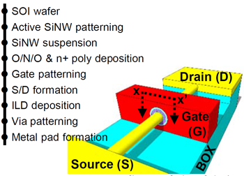
Figure 1. Fabrication of the SONOS device. (SiNW = silicon nanowire; ILD=inter-layer dielectric.) (Image courtesy IEDM – Click to enlarge)
This gives them a device sitting on (and over) the BOX, which itself covers the thick bulk silicon underneath it. And the transfer begins.
At the start of the transfer, the circuit sits atop what is effectively a handle wafer: the bulk silicon serves no purpose except to provide structural integrity. The circuit is going to end up sitting on plastic, so all that bulk silicon has to go. In order to maintain some structure, they covered the top with a protective layer (they didn’t say what this is) and then put a handle material over that (also a mystery). The only thing they really say about this is that this handle can be released by heat.
So now a top handle is in place, and the bulk silicon on the bottom can be etched away, stopping when the BOX is reached. By etching, the oxide becomes a natural stop (which wouldn’t have worked if grinding). They then placed the device on a 35-µm-thick polyimide film and removed the top handle and protective layer. (I’m assuming they had some way to secure the circuit onto the plastic film, although they don’t discuss that…)
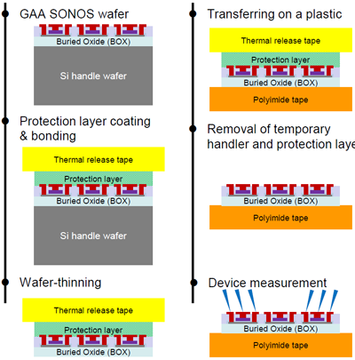
Figure 2. Transfer of circuit from silicon substrate to plastic substrate. (Image courtesy IEDM)
And now, the 64-million-dollar question: Does the memory still work? We actually need to be more precise here, since there are two questions: Does the transfer process degrade performance? And, once transferred, does bending the flexible substrate (further) degrade performance?
The short answers appear to be No and No. Transistor performance changed minimally, if at all, between the silicon substrate and the plastic substrate as well as when bending with a 5-cm and a 1-cm radius.
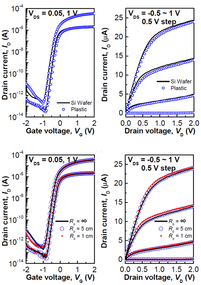
Figure 3. Performance before and after transfer (top graphs) and when bending (bottom graphs). (Images courtesy IEDM)
They then did programming and erasing under these conditions – and maintained a 10-year data retention, with endurance exceeding 10,000 cycles. In other words, they claim that, even after transfer, even while bending, they still have a non-volatile cell that meets industry-standard specs.
They also calculated the strain that bending with a 1-cm radium might place on the device: they came up with 0.1%. This depends, of course, on where the critical silicon bits are in the final assembled stack. There’s this thing called the “neutral plane”: it’s the level right in the mechanical middle. If the material bends down on the sides, then above the neutral plane, the material stretches; below, the material compresses. The farther up or down, then the more tension or compression.
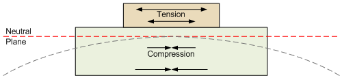
Figure 4. Tension and compression are minimized near the neutral plane when bending.
So keeping the sensitive parts close to the neutral plane minimizes the stresses and strains on the electronics. That means not stacking this on a thick layer of plastic, or else the neutral plane will be somewhere deep in the plastic, not near the electronics.
There’s one more thing I wanted to check out myself. I mean, a 1-cm bend is significant – part of me finds it amazing that brittle silicon can withstand that. But then again, the cm-regime is orders of magnitude bigger than the nm-regime of the transistors. And I suspected that it would be analogous to us on the earth: the earth is round, but on the scale of our existence, it feels flat.
So I scratched my head and did some calculations (you can confirm or find error below) to see what the angle of deflection is on the silicon nanowire. My guess was that it would be much less than it looks when you cringe at a bent circuit.
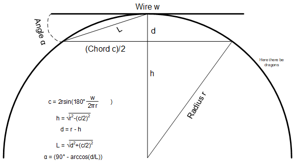
Figure 5. Calculating the angle of deflection of a nanowire. Very much not to scale.
With the radius at 1 cm and the length of the wire at 100 nm, the angle of deflection comes out to… 0.00014° by my calculations. And this is worst-case, as if the entire angle came from a single deflection point. In reality, the angle that any individual point experiences is less, since that total angle is distributed along the arc of the bend, gradually, not all at once.
In other words, at that scale, it really does feel pretty much flat to the wire.*
So this would suggest that a 1-cm bend leaves some margin – although the important calculation is the strain one, which establishes where fracture would occur – it’s somewhere around a half a centimeter bend radius, according to the team. Which means that our impressions of metal and silicon being brittle are actually pretty accurate: at a 0.5-cm radius, the angle of deflection is 0.0003° – hardly anything, and this is where it can break.
So after all is said and done, it’s not so much that thin materials become more flexible (perhaps they can if they are even thinner); it’s more of what we might call a “flat-earth” effect that makes this work.
So, thanks to that flat earth, we may well be able to create flexible electronics out of brittle components.
*I reran various numbers to see how tight a bend would be required to get a 1° angle – and it was on the order of a micron! That made me suspicious as to whether I was doing this right, but then I plugged in a radius that corresponded to the picture above – which would mean a 75-nm radius (as drawn, it’s shorter than the wire– for convenience). And the result comes to 19° – consistent with how it looks in the figure. The figure below shows a 1x wire on an arc of 10x radius, analogous to a 100-nm wire on a 1-µm-radius arc; the wire still looks pretty flat at that scale. (I actually experience an optical illusion that makes the red straight line appear curved along the arc – which it isn’t.)
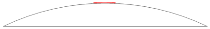
Figure 6. 1x-length wire on an arc of 10x radius. Negligible deflection.
More info:
Flexible High-performance Nonvolatile Memory by Transferring GAA Silicon Nanowire SONOS onto a Plastic Substrate (or session 27.6 in the IEDM proceedings)


Do you think this is a useful approach to creating high-performance flexible electronics?