3D has been tossed about quite a bit over the last few years. We can ignore the 3D TV craze that came and went like an evanescent avatar. But the two IC manifestations have been 3D transistors (i.e., FinFETs) and 3D package integration – stacking chips.
The latter is a more-than-Moore technology that allows multiple chips, each built on processes best suited to it, with the ability to leverage high-volume off-the-shelf dice like memories instead of designing them from scratch.
But what if you want to scale like circuits vertically? That’s to say, things that aren’t available off the shelf and that all require the same process? Either you have to build them laterally on a single chip or build multiple chips and stack them.
Well, Leti is working on another option: monolithic 3D integration. What this amounts to is building a standard chip and then growing a new layer of silicon (or something) above it and building more circuits. Sounds pretty straightforward in concept, but it’s easier to visualize than it is to accomplish. They presented their status at the recent Semicon West gathering.
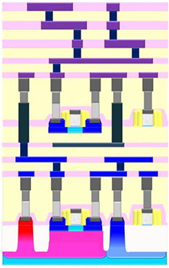
Image courtesy Leti
The biggest concern that always arises with these sorts of ideas is thermal. For the bottom layer, you build your transistors, implant your dopants, and then “activate” them using heat to get them moving to where they’re supposed to be. After that, you want them to stay there. They’ll keep moving if you keep the heat on, so once they’re set, you don’t want any more heat.
There are also apparently worries about the contact salicide stability in the presence of extra heat.
And where might the extra heat come from?
Well when you build the next layers of transistor, you need to dope them and activate again. If your bottom transistors are already where you want them, the extra activation will screw them up. Do you try to under-activate the bottom ones, hoping that the second activation will bring them in line?
That’s not the approach Leti is taking. They’re experimenting with a “crème brulee” technique: use a broiler for the second layer activation. That is, heat from the top so that only the top layer gets activated in a short enough time that the heat doesn’t diffuse down and mess up the lower transistors.
Compatibility with existing processes is another consideration. You have to be able to connect the upper and lower transistors, and, in theory, there is no such interconnect at present. Rather than define new interconnect, they’re leveraging the local interconnect (LI) for that piece.
Finally, a big question: how to build and arrange the transistors and CMOS pairs – and other elements like NEMS devices that might want to ride along on the same chip? They’re playing with three different configurations.
The first is “CMOS over CMOS.” In other words, you build both N and P types on the same layer (top and bottom). They list FinFET over FinFET, Trigate/nanowire over Trigate/nanowire (all SOI), or FDSOI over FDSOI. But they also have a drawing showing an FDSOI transistor over a FinFET. Their allegation is that two layers of 14-nm technology provide the scaling of a single layer of 10-nm technology.
The second option is to optimize the transistors by having N and P types on different layers. So, whereas the first option has CMOS pairs built laterally, they’re built vertically in this second option. This allows them to use different materials on the two layers. They’ve already tried germanium (Ge) for P over silicon for N. And they’ve leveraged different crystal orientations, with silicon [110] for P over silicon [100] for N. Next up they’ll try InGaAs for N over Ge for P.
The third option involves integrating NEMS over CMOS. We looked at their M&NEMS program last year (which work continues).
They did some FPGA work already just to see what kinds of improvements they can get . They used two stacked FDSOI layers and two levels of tungsten LI. They improved area by 55% (not surprising), but they also improved performance by 23% and power by 12%. Win win win. Apparently going local matters.
We’ll update as we see new results.