AI/ML rules at the 2024 SPIE Advanced Lithography + Patterning symposium

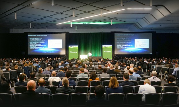
The SPIE Advanced Lithography + Pattering symposiums were held from 25-29 February this year with enthusiastic and sizable attendance. The research presented at SPIE has fueled advancements in semiconductor manufacturing for 40 years. As always, the Calibre Manufacturing group was well represented with two invited papers and another 16 session papers.
Our first invited paper, titled “An artificial intelligence machine learning (AI/ML) approach with cross-technology node learning for multi-layer process defect predictions” described a new defect prediction flow using a feature-based artificial intelligence/machine learning tool. This tool uses previous technology process improvement data to generate predicted defect patterns for a new technology. The paper was developed with Advanced Micro Devices (AMD) and presented by Jonathan Ho of AMD.
Our second invited paper, “Machine learning (ML) based SEM contour extraction accelerated by GPU for etch modeling application,” introduced a method of extracting contours from a variety of SEM images using a deep learning model and using GPUs to speed up the process 20x. It was developed jointly with IME and presented by Yuansheng Ma of Siemens EDA.
The 16 other papers delved into a variety of topics like model-based OPC, curvilinear mask technologies, EVL, directed self-assembly, metrology, edge placement error, wafer defect detection with ML, using ML to improve design sampling, cloud computing for post-tapeout flows, and more.
For more details on the papers we presented, plus additional resources, visit Calibre IC Manufacturing papers at SPIE 2024.
The head of Calibre Manufacturing Solutions, Steffen Schulze, participated in a panel hosted by Applied Materials. “Patterning in the Angstrom Era: It Takes an Ecosystem” focused on the changes coming across design, process and control. A key topic was the introduction of high NA EUV lithography. Steffen said that chip architects are looking to the ecosystem to deliver field stitching without any design impact or special design rules for that area. “That’s a very challenging task,” he said. “We know it will require more aggressive resolution enhancement techniques. It may require special mask rules in these areas.”
Siemens EDA also partnered with SPIE to present the annual Nick Cobb Memorial Scholarship to Mr. Nicholas Jenkins. The scholarship honors Nick Cobb’s fundamental work in the field of lithography and his many contributions as the chief architect of the Siemens EDA Calibre OPC solutions.
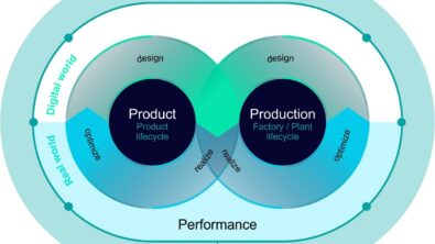
Other notable events at SPIE included a tribute to industry icon Gordon E. Moore, who died last year at age 94. The plenary session the following day from Ann Kelleher of Intel talked about the new era of Moore’s Law depending on system-technology co-optimization (STCO), which is needed in addition to design technology co-optimization (DTCO). Learn about the Calibre approach to extending DTCO in our technical paper, Extending design technology co-optimization from technology launch to HVM with Calibre Fab Solutions.