

If you’d asked me a year ago (or two, or three) what I thought about Xilinx’s cost-optimized device offering, I’d have told you that I firmly believed that the company had given up on the low-cost FPGA and programmable logic market, leaving it to other, more eager competitors like Lattice Semiconductor and Microsemi/Microchip. Intel (formerly Altera) had been maintaining parity with Xilinx on low-cost abandonment, with both companies offering the same basic devices they’ve had for several years, not really putting any marketing or visible engineering energy into that market, and focusing instead on competing with each other in high-performance applications targeted at the data center.
We questioned the wisdom of letting go of the cost-optimized market. With the rapid build-out of IoT with demanding applications at the edge, including the need for acceleration of AI inference and other workloads, it seemed that the edge acceleration market was poised for a rapid expansion, with FPGAs being an ideal solution for many markets. Why would Xilinx walk away from such a potential gold mine in order to focus exclusively on challenging Intel’s dominant position in the data center?
Well, turns out they didn’t.
Xilinx has just rolled out a set of new and unexpected highly-competitive and well-positioned devices – both FPGAs (Artix) and SoCs (Zynq). The new families – based on current process nodes and with modernized sets of peripherals and interfaces – are guaranteed to cause heartburn for competitors who have been playing aggressively while the cat was away. Well, the cat is back and it may be time to fortify those mouse holes.
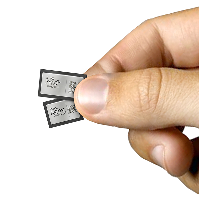
Newly announced are a smaller, cost-optimized member of the Zynq SoC/FPGA family (Xilinx simply calls Zynq an SoC, but their primary differentiation is their on-chip FPGA fabric integrated with a multi-core ARM processing system and beefy I/O. The new Zynq and Artix devices are built on Xilinx’s UltraScale+ technology base, fabricated on TSMC’s 16nm process – offering significant improvements in performance-per-watt, form factor, and thermals, as well as scalability across Xilinx’s entire UltraScale+ portfolio from high-end Virtex, Kintex, and Zynq devices down to the smallest new offerings.
On the Zynq front, Xilinx heard a lot of demand for a smaller device that would use less power and fit in smaller form factors but still deliver the needed performance and features for edge applications. In response, they designed the new ZU1, which scales back the amount of programmable logic fabric and memory a bit, while maintaining the IO, DSP, and ARM processing system sizes. The result is a device that uses 40% less power (with only 20% less programmable logic fabric). The device has a “deep sleep” mode that allows selective power-down of islands resulting in a minimum static draw as low as 180 nanowatts.
The new ZU1 includes 2 or 4 Arm A53 MPCores, 81K logic cells, 38 Mb block RAM, 216 DSP slices, 2 USB 3.x and 4 Gigabit Ethernet ports, and a ton of IO – all delivered in new UVBA packages at 9.5 X 15mm with 0.5mm ball pitch. This makes the ZU1 attractive for a wide range of applications where its larger siblings were just too big or too power hungry, and it enables a new category of size- and power-optimized SoCs with built-in acceleration capability.
The new Artix family benefits heavily from the UltraScale+ process (vs the 2-generation older 28nm of the previous Artix family). Xilinx has also piled on the features, including 16Gbps transceivers, hardened crypto/security blocks, DPA resistance, and a bunch of DSP blocks. The result is up to 192 Gbps aggregate bandwidth, even on the smallest device. Artix is also updated with support for emerging protocols in vision, video, networking and storage.
Competitively, Xilinx claims the new Artix family delivers best-in-class capability in SerDes data rates for advanced protocols (including PCIe® Gen4), highest DDR memory performance (DDR4 – 2400), highest MIPI performance for the latest vision sensors (“4K/8K Ready” at 2500Mbps), and highest max DSP performance (775 MHz, 1860 GMACs, 620 GFLOPs). That makes these devices ready to tackle a wide range of applications such as image & video processing, real-time control, and AI inference – in situations that demand small form factors and low power consumption.
The new Artix family includes four devices, ranging from 96K to 308K logic cells, 3.5Mb to 10.5Mb total block RAM, 400 to 1,200 DSP slices, PCI Gen 4 (planned) on the smaller 2 device and PCI Gen 3 (released) on the larger 2, and twelve 16Gbps SerDes transceivers on every device.
One of the biggest innovations in the new families is in packaging technology, where Xilinx is taking advantage of new Integrated Fan-out (InFO) packaging to deliver devices that require 60% less PCB area and are 70% thinner. This improves everything from signal integrity to thermal performance and saves a lot of PCB real-estate (as long as you are ready to handle the 0.5mm ball pitch). Combined with the other benefits, this puts the new Artix and Zynq devices in a whole new category for consideration in edge device applications. It also places them in a unique corner of the compute-density-per-area map, differentiating them significantly from alternative architectures.
The scalability, granted, sounds like so much marketing hype, but it does deliver significant value when your team is re-using design across a range of products with varying capability levels. The design you made for a high-end Virtex application should move pretty seamlessly to a scaled-down version on the new Artix. Or, producing a cost-power-optimized version of a design running on a larger Zynq chip should be a snap when moving to the new small-but-peppy ZU1.
The new Zynq devices will have early-access tools available in March, and the ZU2 and ZU3 devices are in pre-production now, with production in Q3. ZU1 will be ready for pre-production in Q3, with full production in Q4 of this year. Artix is on a similar schedule, with documentation available Q2, tools in Q3, the two larger devices (AU20 and AU25) in production in Q3, and the two smaller devices in pre-production in Q1’22.
It will be interesting to see how these new Xilinx devices affect the cost-optimized programmable logic landscape and the potential rapid expansion of sockets that can be served with programmable logic in edge-based devices.


