

I just had something of an epiphany.* What pops into your mind when you are exposed to the term “extreme edge”? Assuming you are of a technical nature, I’d wager the first thing you consider is the “things” portion of the internet of things (IoT). That is, the smart connected sensors and actuators that sit at the interface between the network and the real world. My epiphany, such as it was, is that another way of looking at the extreme edge is from the perspective of those entities in the real world that interface with the aforementioned “things.” Taking this one step further, I am one of those entities, which means I’m living at the extreme edge. Hmmm. This may go some way toward explaining my increasingly nervous disposition. (*I didn’t say it was a great epiphany).
On the one hand, I think artificial intelligence (AI) is awesome (I can only hope our future AI overlords will take note of this sentiment come judgment day). On the other hand, it must be acknowledged that AI comes at a cost. What I laughingly refer to as my mind is currently reeling at some of the numbers to which I’ve recently been exposed. For example, training the ChatGPT-3 model reportedly generated over 500 metric tons of carbon emissions (I’m scared to ask about ChatGPT-4), which equals the emissions of over 600 flights between London and New York. Furthermore, it’s said that the carbon footprint of a single AI query could be 4-5 times that of a typical search engine query. With daily consumption estimated at 1.17M GPU-hours, equating to 150K server-nodes-hours, ChatGPT reportedly emits about 55 tons of CO2 equivalent daily, which is comparable to the lifetime emissions of an average car.
The reason I’m waffling on about all this is that many of the people I’ve been chatting with recently have been telling me how they are moving artificial intelligence (AI) and machine learning (ML) out from the data center to the edge. So, you can only imagine my surprise and delight when I was introduced to Moshe Tanach, who is the CEO and Co-Founder of NeuReality. Moshe informed me that NeuReality’s AI play remains in the cloud. The mission of the folks at NeuReality is to make AI easy, to democratize AI adoption, to increase AI performance by 10X, to reduce AI infrastructure cost by 10X, and—as an added dollop of allegorical whipped cream on top of the metaphorical cake, to mitigate the carbon footprint associated with using AI. And, for their next trick…
I’ve said it before, and I’ll doubtless say it again—I’m a simple man. Wait, there’s more! What I mean to say, if you’ll let me finish, is that I’m a simple man and I like a simple story that I can wrap my brain around. The story Moshe told me is simple at its core, which is not to say that NeuReality’s holistic hardware and software solutions aren’t incredibly revolutionary and sophisticated (their mindboggling complexity is happily hidden “under the hood”).
Let’s start with the fact that the folks at NeuReality don’t concern themselves with the training of complex AI models. Instead, the focus of their attention is on optimizing the use of trained deep learning models and inferencing engines deployed in the data center. Let’s set the scene by considering CPU-centric inferencing architecture as illustrated below.
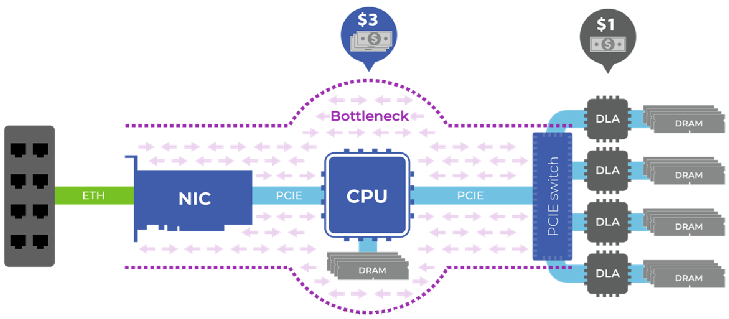
A CPU-centric inferencing architecture causes increased cost and power consumption and lowers efficiency (Source: NeuReality)
This reflects a typical inferencing server that serves (no pun intended) as an Alexa backend server or a recommendation engine server or something else of this ilk. The CPU is a high-end (read “expensive”) beast from Intel or AMD. The deep learning accelerators (DLAs) are where the AI inferencing takes place.
All of the requests coming into the server arrive through the internet and land in the CPU, which now needs to perform a bunch of tasks to prepare the job to be handed over to the DLA. If the task involves face recognition, for example, the images being fed to the system will arrive in compressed format, so they will need to be decompressed, resized, and processed in other ways before being passed to a DLA. These tasks load down the CPU, which ends up being the bottleneck in the process.
As the first step in addressing this problem, the guys and gals at NeuReality created a new class of device they call a network addressable processing unit (NAPU) because it’s directly connected to the network. Look at the diagram below. Count the CPUs. That’s right… there aren’t any!
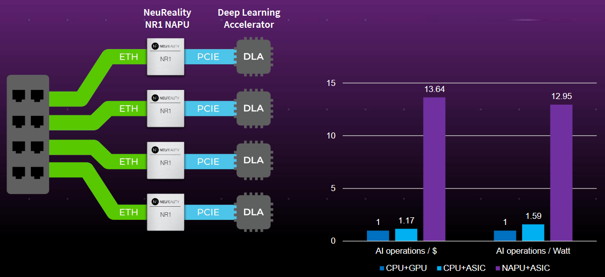
NeuReality’s AI-centric technology reduces AI infrastructure costs by 10X (Source: NeuReality)
Observe the bar charts on the right of the above image (for ASIC and GPU read “DLA”). The NAPU+ASIC combo offers 10X AI operations per $ and 10X AI operations per watt as compared to its CPU+ GPU and CPU+ASIC competitors (more details about these benchmarks are available on the NeuReality website).
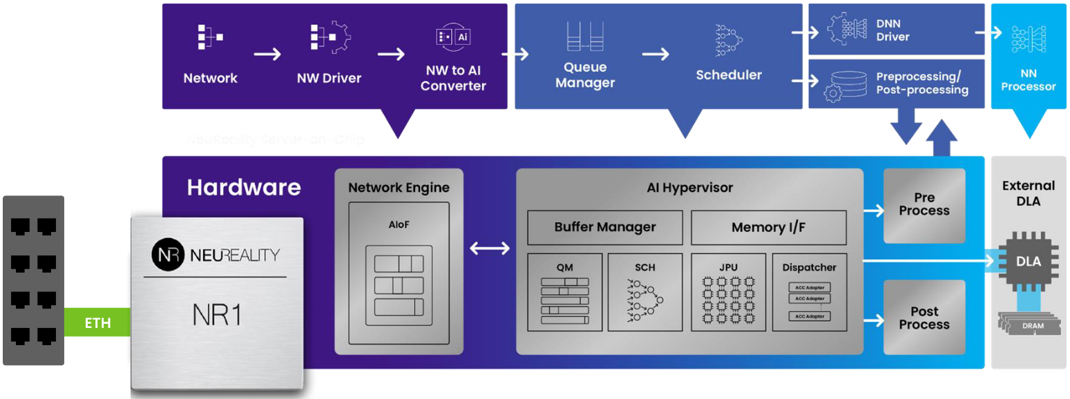
High-level view of the NR1 (Source: NeuReality)
The NR1 NAPU does everything in hardware, including the network termination and communicating with the client side that sends the images or the text. It also does all necessary pre- and post-processing, and everything is all based on a compiler developed by the chaps and chapesses sporting “I LOVE Working at NeuReality” T-Shirts.
Consider an inference model that’s been trained in a PyTorch or TensorFlow framework. You use NeuReality’s tools to take that model and compile it for use on the DLA. Whichever DLA company you are working with (NVIDIA, Qualcomm…), NeuReality provides a common interface, connecting to the DLA company’s deep learning toolchain.
It’s important to note that NeuReality doesn’t provide only a hardware plane—instead, they supply a system plane that features three layers of software. The first supports the model. The second covers the pipeline (the piece that does the pre- and post-processing. And the third is the service that connects automatically to Kubernetes for management, orchestration, and provisioning.
It’s also important to note that the NR1 NAPU is but one of a trio, a tried, or a troika of offerings. The NR1 NAPU is used to power the NR1-M PCI Module, which is itself used to power the NR1-S Server.
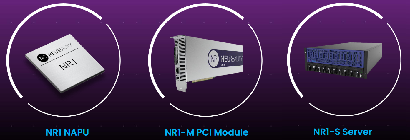
A trio, a tried, or a troika of offerings (Source: NeuReality)
Let’s take a slightly closer look at the NR1-S server, as illustrated below. Observe that this flaunts two rows of cards. The cards at the front of the server (on the left in this diagram) are NR1-M modules. The cards at the back of the server (on the right in this diagram) are the DLAs of your choice.
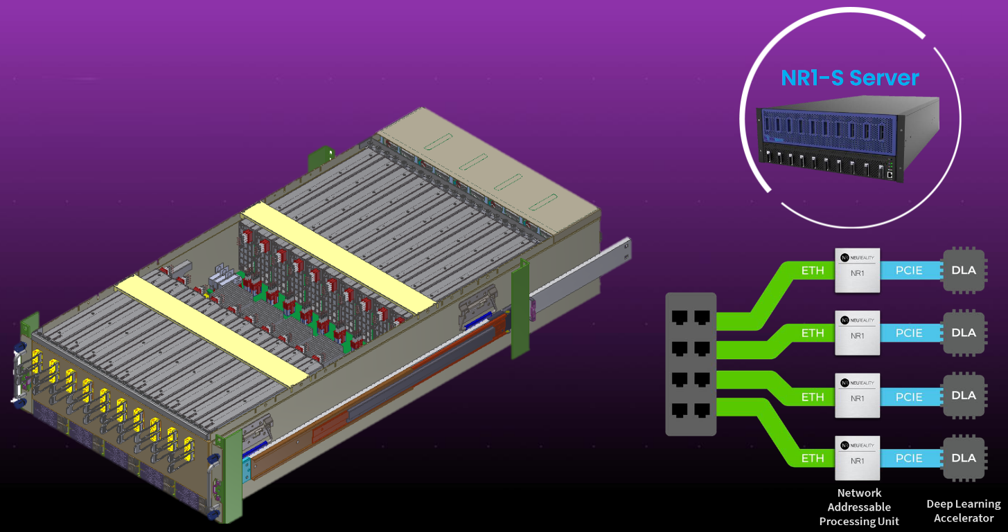
Meet the NR1-S AI-centric server (Source: NeuReality)
I tend to get a little confused by the business side of things, but my understanding is that NR1 NAPU chips are a fraction of the cost of the high-end CPUs found in data center servers. Similarly, the combination of NR1-M modules with DLAs is much more cost-effective and efficient in terms of AI operations per ($, watt, or other metric of your choice) as compared to traditional offerings.
Consider how much of a data center’s activities are devoted to AI inferencing today and how much more is going to be the case in the not-so-distant future. NeuReality’s technology is going to dramatically reduce the capital expenditure (CapEx) and operational expenditure (OpEX) associated with these activities, which will be music to the ears of the data center’s owners and users.
I’m not an expert in this area (or any other, if the truth be told), but NeuReality’s technology is a new reality for me (I’m sorry… I couldn’t help myself). I’ve not seen anything quite like this before. It seems to me the folks at NeuReality may have created a new market niche, which they’ve also filled with some very interesting solutions. I expect to see great things emerging from all this. How about you? Do you have any thoughts you’d care to share regarding anything you’ve read here?


2 thoughts on “Want to Reduce Your Data Center AI Inferencing Infrastructure Costs by 10X?”