


Soooo… you’ve decided you’re going to create a system-on-chip (SoC) device of such awesomeness that it will leave your competitors gnashing their teeth and rending their garb. You’ve also decided to base this on a RISC-V processor. What you want is the biggest, baddest RISC-V processor going. Furthermore, you want this processor to be customized to allow you to take full advantage of your own “secret sauce” IP. Who ya gonna call?
I’ll give you a clue, which is that the Ghostbusters aren’t going to be of much help in this case. But turn that frown upside down into a smile because the guys and gals at Semidynamics Technology Services are ready to leap into action.
I was just chatting with Roger Espasa, who is the Founder and CEO at Semidynamics, and I now know more about customizing RISC-V cores than I ever expected.
Just to provide a little background, Semidynamics was founded in 2016. The folks at Semidynamics spent the first two and a half years offering design services before transitioning to offering IP. Although they are based in Europe, they also have customers in the US and Asia. In addition to their customizable RISC-V processor cores, they lay claim to offering the only and biggest out of order (OOO) RISC-V vector unit.
Yes, of course you are correct. If they are offering the only OOO RISC-V vector unit, then it is—by definition—the biggest, but dare I suggest you are being a tad pedantic to point this out?
The Semidynamics business model is reasonably standard. If you request any changes to the cores, you will be charged NRE accordingly. Once any such customizations have been implemented, you will be provided with a corresponding bitstream for the FPGA of your choice, thereby allowing you to verify that your spiffy new custom core is all you wanted it to be. If you are happy (and Roger says that, thus far, their customers have always been happy), you’ll sign a license to tape-out, they will give you the RTL for your core, and they will support you all the way through the tape-out process (their cores have been implemented at the 22, 12, 7, and 5nm process nodes).
Before we plunge headfirst into the fray with gusto and abandon (and aplomb, of course), let’s start by briefly introducing four names and icons as follows:
![]()
Meet the processor cores and related technologies (Source: Semidynamics)
If you just need a regular mid-range-performance processor, then the 64-bit in-order Avispado—which means smart, fast, and witty in Spanish—is the one for you. This is available as a 2-wide processing unit, which means it can perform two operations on each clock.
By comparison, if your application demands more extreme processing capability, then you will want to be looking at the 64-bit out-of-order Atrevido, which means daring, courageous, and bold in Spanish. This bodacious beauty is available in 2-, 3-, and 4-wide configurations.
High-level block diagrams for the Avispado 223 and the Atrevido 423 are shown below. As opposed to many companies’ numbering schemes—the attempted understanding of which makes one’s brains leak out of one’s ears—the approach adopted by Semidynamics is a delight. In addition to the fact that the Avispado and Atrevido monikers immediately inform that you are talking about in-order or out-of-order, respectively, the first number specifies the width while the last two numbers indicate the year, so the Avispado 223 is an in-order 2-wide processor that was presented to the market in 2023, while the Atrevido 423 is an out-of-order 4-wide processor that bid the market a cheery “hello” in 2023.
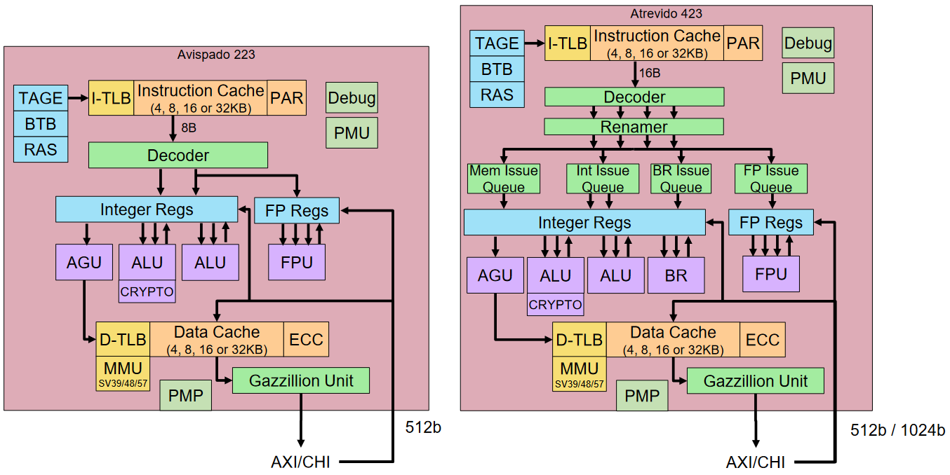
High-level block diagrams for the Avispado 223 (left) and the Atrevido 423 (right) (Source: Semidynamics)
Both of these processors are available in two flavors—with an AXI interface for people who don’t need coherency and with a CHI interface for those who do. Both processors include a Gazillion Unit (shown in the block diagrams above), which dramatically improves memory accesses. And both processors can be augmented with the aforementioned OOO vector unit (not shown in the diagrams above, so you can stop looking for it). We’re on a roll here because both processor types also offer the following:
- User, Supervisor, and Machine privilege levels.
- Hypervisor available in Q4 2023
- Linux-ready memory system with a memory management unit (MMU) (supports SV39/48/57), coherent caches with parity of ECC, and hardware support for atomics and unaligned accesses.
- PMP regions (0 to 16).
- Advanced debug capabilities (RISC-V debug spec compliant interface over JTAG and HW/SW breakpoint support).
- RISC_V extensions supported: Vector, Crypto, Bit Manipulation, CMOs, Zifenci.
- Quad-core ready.
Roger says that, like other vendors, the folks at Semidynamics can easily change obvious things like cache sizes and bus sizes. Where Semidynamics differentiates itself is that they are willing to make much more complicated and radical changes. For example, if you want to connect something right in the middle of the MMU unit to implement some funky loads that do “I don’t know what” for your special computing needs, the team will happily do this for you (this is why they describe themselves as being “Experts in open core surgery”).
Observe the Gazillion unit in the block diagrams above. Roger says this is something that they’ve worked very hard on. The idea is that we want the core to stop as little as possible and Gazillion helps to avoid latency issues when accessing off-chip memory. In contrast to traditional processors, which employ a “stop-and-go” operating mode when encountering multiple cache misses, Gazillion technology allows the processor to send up to 128 requests to the memory system, thereby allowing the processor to continue to do useful processing while previous misses are served. To put this into perspective, the figure below compares the Gazzillion technology in the Atrevido and Avispado cores to other popular cores available in the market.
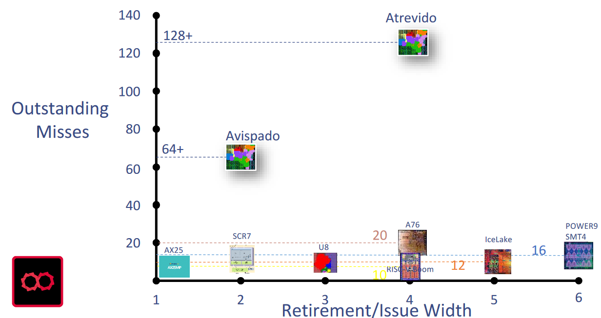 Gazillion compared to other CPUs (Source: Semidynamics)
And so, finally and inexorably we find ourselves at the point in our discussions when we turn our attention to the optional OOO vector unit we made mention of earlier. Let’s start by noting that this little rascal is 100% customizable according to your needs. Customization #1 is to choose between V4, V8, V16, and V32 options, which have 4, 8, 16, or 32 vector cores, respectively.
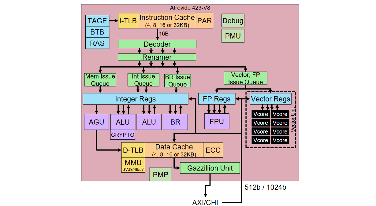 Atrevido 423 + V8 Vector Unit (Source: Semidynamics)
Customization #2 is to select the data types you wish to support out of INT8, INT16, INT32, INT64, BF16, FP16, FP32, and FP64. If your SoC is intended for high-performance computing, then you’ll probably want your vector unit to support the whole shebang up to and including FP64. If Oil and Gas is your bag, then FP32 and its friends may be all you need. Or, if you are more focused on artificial intelligence (AI) and machine learning (ML), it may be that FP32 and INT8 will suffice.
But wait, there’s more, because Customization #3 lets you decide on your vector register length—options are 1X, 2X, 4X, or 8X the number of vector cores—which is great when it comes to increasing performance and reducing power consumption.
One last point here is that you may wish to connect the vector unit to your own “secret sauce” IP block, but you don’t want to share any information as to what’s in your IP. No problemo, because the folks at Semidynamics provide a very simple protocol they call their “Open Vector Interface” that allows you to do your “thing” without telling anyone else just what it is you are doing.
There’s so much more to all of this, but I fear I cannot do it justice, so if you wish to plunge deeper into the techno-details, please reach out to the folks at Semidynamics (don’t forget to tell them that “Max says ‘Hi’”). In the meantime, as always, I’d love to hear any thoughts you’d care to share in the comments below.


There is just one thing missing. How do you get all the data from memory to feed all these paper tigers…that is in addition to get enough instructions from the same memory to pile up waiting for data in all this exotic hardware?
I am a novice that started in the ANFSQ7/8 (SAGE air defense system) July 15, 1957. The best solution at that time was Interleaved Memory. There could be an outstanding request to an odd and an even memory address to feed the overlapping decode/execute cycles.
Then System360 came to be and the high ends processors had 4 way interleaved memory access. (Models 65/75/91). Mod91 was tuned for matrix inversion where Bob Tomasulo(spell check) came up with out-of-order execution etc. And Cache had not been conceived until the 360/85 came to be.
All of this was “Intuitively Obvious” as there was no way to measure CPU performance in a meaningful way. Well we are 50+ years in the future and not much has changed. That is except for the fact that Super Scaler and Both instruction caches data/instruction are mandatory. Aw, it doesn’t matter if that crap is overrated … Gotta Have It!
A little aside here: Since there was no known way to measure computer speed meaningfully, for comparison purposes of design alternatives “Cache hit ratio was assumed” and used to compare alternative designs. Those were assumed numbers that noe have been accepted as real measurements.
So here we are with something 50 years old that is new again [RISCV] and it is going to save us. Not to mention that multiply was immediately added and now Vector instructions are must haves.
So I will quietly ignore all of this nonsense until “they” (anybody) can explain how they get all the instructions and data piled up and waiting for the magic to happen.
I remember interleaved memory from my days designing mainframes — re your questions, I will ask them to comment — they did explain all of this in excruciating detail but I am a bear of little brain and a lot of it went over my head (said Max, sadly)
“Gazillion technology allows the processor to send up to 128 requests to the memory system, thereby allowing the processor to continue to do useful processing while previous misses are served.”
Wow, time to find that memory system and pen an article about it!
Meanwhile , if you are interested in something real, open source, working, take a look at the C#(Roslyn) API. At the heart of it there is an AST(Abstract Syntax Tree), Syntax visitor(Syntax walker), and compiler.
In short, “what guzzinta” is source code — if/else, for, while, do, and expressions.
“what cumzoutta” is a sequence of nodes, just old numeric, variable, add, sub, mpy, assign, etc.
So first, stuff the numeric and variable values into full dual port memory embedded memory (so operands can be read at clock speed), pass them thru the ALU, write the intermediate result into the stack(which is another dual port) then when all operators are processed, write the result into the destination variable.
In all, this will take about 3 embedded memories, less than 1,000 LUTS on an off the shelf FPGA. No exotic memory system need apply. Ya know it’s kinda like “ya send the data to an accelerator and read back the results”.
Is this “RISCy” enough?
It’s risky enough for me LOL
Here is a quote from the website:
“In contrast, Semidynamics Gazzillion™ technology allows the processor to send up to 128 requests to the memory system, whereas other cores can only tolerate very few cache misses. This means that the processor continues doing useful processing while previous misses are served. The figure below shows how up to 128 misses can be sent to the memory system before the processor stalls waiting for memory accesses to complete. In this case, the idle time is reduced to almost zero, because the stop happens very close to the time the first cache miss is resolved.”
For this to be the case, there would have to be a backlog of data fetched before the first cache miss. This means that the memory read data faster than the processor could process it.
Reminds me of the old “prefetch” game that never worked because there never has been a case that memory had enough bandwidth to deliver data faster than the processor could process. Here we are talking about a cache miss (which probably estimated to be 5% cache miss to hit ratio) which illustrates the point that caches fetch a “line” of data rather than a word because it is intuitively obvious that data is processed within a small range of consecutive addresses.
In the real world empty blocks of memory are allocated. Data then has to be put into that empty memory before it can be used, duh? In today’s FPGAs there are hundreds of embedded memory blocks that no one seems to know how to use. Seems to me embedded memory should be allocated so data could be fetched from local dual port blocks instead of memory….and no more cache misses and wild and hairy algorithms.
Hi Karl — I’ve asked them to respond to your questions here in the comments — I look forward to hearing what they say 🙂
Hope I am wrong…
I am waiting. (not with baited breath)
Most of this crap dates back to the System360 Mod91.
— which was not a general purpose machine. It was honed, tuned especially for something called matrix inversion. Cache had not been invented, virtual memory had not been invented. It was pre-deceased by something called Stretch.
I once attended a presentation by Dr. Fred Brooks who was deeply involved in Stretch and System360.
H said that they put everything they could think of in Stretch — “it even had Gargoyles”.
The Mod91 was not general purpose but had been developed as a “Scientific” exception.
But it had out of order execution and whatever else that was necessary to be called “Super Scaler”.
And as Professor Dijkstra noted “complexity is what sells”.
So here we go again around the mulberry bush!!
Professor Dijkstra invented the Shunting yard Algorithm which is key to handling operator precedence in expression evaluation. But we are stuck with HLS/SystemC that have been “maturing” for 20+ years.
I am so glad they were so eager to reply.
Shoot — I thought they had replied — I will “tweak” them again soundly.
I just heard back that “Spain closes down in August” plus there’s a big RISC V show coming up in China, but I’ve asked them to respond as soon as they can.
Thanks Max. By the way, quite sometime ago I started out to get a project up and running to send to you. Wellll………… I am working on it but false starts are getting in the way. Later.
No worries — no rush — I’m currently working 7 days a week so I have little free time anyway (sob sob)
I really don’t care and since I am the only one out here in the cold, I hope they have fun and sell a zillion.
“I hope they have fun and sell a zillion.”
Me too because they are really nice folks (when you can track them down 🙂
Hi Karl,
I will try to explain the utility of Gazzillion in a bit more detail.
The scenario for which Gazzillion is designed is an application with a very low hit rate in the cache. For example, a “memcpy” subroutine that is copying an array of 1MByte of data from buffer A to buffer B. Neither buffer A nor buffer B will be cached in the 32KB L1 cache (they are both together 2MB worth of data, so the probability of finding any cache lines belonging to either buffer in the L1 cache is very low). In this scenario, the OOO core has enough out-of-order depth to unroll a memcpy loop (including its vector instructions) multiple times. If you only had one cache miss outstanding from the L1 cache to the memory system, the OOO capabilities would not be very useful. After the first cache miss, the whole processor would eventually grind to a halt. In contrast, Gazillion supports up to 128 independent cache misses to the memory system. This allows the processor to fetch the data wanted (note, this is not a blind prefetch, i.e., the processor is not “guessing”, it unrolled the loop so it knows exactly which cache lines it wants) and tolerate the latency of the next level of the memory hierarchy. As the data returns, the processor consumes it (never faster than it returns, of course). The goal of Gazzillion is to support applications with very large data sets, which have low chances of hitting the L1 data cache.
Hope this clarifies things a bit 🙂
Thanks, maybe yes, maybe no. This kind of looks like a cache bypass. Even though the loop was unwound the data is streaming back (DDR) a line at a time. This begs the question “How much of the data used is sequential? ” because if only one word of each line is used most of the bandwidth is wasted.
Or another way of looking at it, Why is there a cache in the first place? Isn’t this just a data pre-fetch scheme? That is more or less the first premise of the cache concept — read a block and hope the hit ratio is high enough so there is a performance gain? It just is not clear that un-rolling the loop overcomes random access limitations.
I will just say “Farewell” and wish you luck.