

It seems we are announcing new AI inference hardware on a weekly basis these days. There is an incredible amount of engineering talent and energy going into the task of developing the next generation of computing architecture – one optimized for the AI revolution. Recently, Untether AI came out of stealth mode and unveiled an entire ecosystem aimed at boosting performance and cutting power consumption in AI workloads in a wide variety of systems, via a PCIe accelerator card boasting a new chip architecture developed by the company.
Let’s look at the chip first.
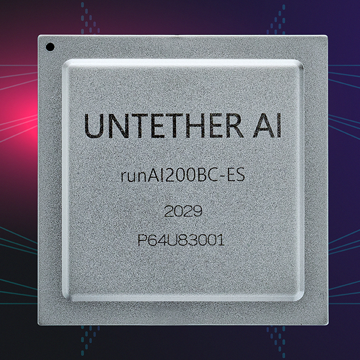
Untether looked at the inference task from a power consumption perspective and observed that a large portion of the power burned by any inference task (a whopping 91% according to Untether) is used to move massive amounts of data in and out of external memories. The company attacked this problem with an architecture they call “at-memory computation” – which really amounts to putting large amounts of memory as close as possible to the location where data will be needed for computation. This is accomplished via a memory bank block containing 385KBs of SRAM with a 2D array of 512 processing elements. There are 511 such banks on the “runAI200” chip, yielding 200MB of highly-localized memory and a beefy 502 TeraOps, in what the company calls “sport” mode. There is also an “eco” mode which maximizes power efficiency, yielding a remarkable 8 TOPs per watt (about the best we’ve seen in this class device).
The runAI200 chip achieves this with a novel architecture, rather than exotic silicon. The company says it is fabricated on a mainstream 16nm CMOS process. In addition to hyper-locality of memory, the performance/efficiency magic includes reliance on integer data types (hence quantization is necessary). The combination of massively-parallel MAC operations, data locality – with on-chip storage of coefficients, and batch=1 optimization gives significant advantages in power and performance.
Tailored for inference acceleration, runAI200 devices operate using integer data types and a batch mode of 1. At the heart of the unique at-memory compute architecture is a memory bank: 385KBs of SRAM with a 2D array of 512 processing elements. With 511 banks per chip, each device offers 200MB of memory, and operating at 960MHz delivers 502 TeraOperations per second in its “sport” mode. It may also be configured for maximum efficiency, offering 8 TOPs per watt in 720 MHz “eco” mode. The new runAI200 devices consist of 19.4 billion transistors, manufactured using a cost-effective, mainstream 16nm process. The architecture appears to borrow several concepts from the FPGA world, including the localized on-chip memory blocks and redundancy – allowing for higher yield.
Diving into some details, the chip is a highly regular structure, and the routing architecture is optimized for inference. There is “direct row transfer,” which is a column-based bank-to-bank local interconnect that provides 32 GB/s transfer for a total of 15 TB/s. Going the other direction is a “rotator cuff,” which provides column-to-column movement of 16GB/s bank-to-bank for a total of 8TB/s. All of this makes its way to and from the PCIe block via a row-based ring pipelined bus that manages 8GB/s per row, for a total of 80GB/s. The PCIe block itself is PCIe gen 4 x16, delivering 32GB/s connectivity. With all that, data can move throughout the chip as well as on and off with minimal friction. The chip also has a specialized 32-bit custom instruction set RISC processor operating at 920MHz to handle housekeeping tasks while the inference fabric does the heavy lifting.
Untether AI puts four of the runAI200 devices onto their “tsunAImi accelerator card” which delivers a crazy 2 PetaOps in a PCIe form factor. The formidable throughput and efficiency of the chip makes this kind of performance possible within the limited form factor. The card manages 1 PetaByte/s memory bandwidth, which can be DMA with the host processor system, maximizing access of the AI engine to application data. The tsunAImi card claims significantly higher performance than other cards we’ve seen, with something like triple the performance of competitors such as Qualcomm, NVidia, Tenstorrent, and Groq – and double the power efficiency of the nearest competitor, despite many of the competitors being built on more advanced (and more expensive) semiconductor processes. Untether claims this can mean a significant savings in total cost of ownership.
Of course, the users have to program the thing, and to do that Untether AI offers the “imAIgine Software Development Kit.” The company says the flow is automated, and it starts with popular and familiar TensorFlow and Pytorch frameworks. There is a lot of model-crunching to do, including quantization, layer optimization, layer-replacement/approximation, and optional post-quantization retraining. The model must then be mapped onto the chip and resources allocated and optimized. To see what you’ve done, the system provides visualizations, including resource allocation and congestion analysis, cycle-accurate simulation, and utilization reporting.
Of course, there is always the question of accuracy retention when quantizing and munging around on models, and Untether claims that (for example) automated quantization on ResNet-50 v1.5 moves accuracy from FP32: 76.458% Top-1 to INT8: 76.298% Top-1. That’s a very small accuracy price to pay for the enormous benefits in performance and efficiency from dropping FP32 in INT8. On MobileNet v1 the company claims we go from FP32: 71.666% Top-1 to INT8: 70.620% Top-1, and UAT: 71.336% Top-1.
Because models will need to be partitioned across multiple chips, there is a heuristic partitioning algorithm that does graph analysis after compilation. It is designed to minimize chip-to-chip communication and is extensible to multiple-card partitioning. This means that the system is scalable to enormous models, which will become increasingly important as the average model size is growing rapidly at this point in our AI evolution.
The runAI200 devices and the tsunAImi accelerator card are sampling now and should be available in production in Q1 2021. It will be interesting to see the adoption of this multi-petaOps solution versus the offerings of some of the more established players.

