

As is usually the case, strange things are afoot in Max’s World (where the butterflies are bigger, the flowers are more colorful, the birds sing sweeter, and the beer runs plentiful and cold). Allow me to expound, elucidate, and explicate — don’t worry, I’m a professional, it won’t hurt at all (well, it won’t hurt me, but you’ll have to take your chances).
The word “pragmatic” is defined as “dealing with things sensibly and realistically in a way that is based on practical rather than theoretical considerations.” The reason I mention this tidbit of trivia is that I recently received an email from Ken Williamson, who is the chief operating officer (COO) at PragmatIC Semiconductor.
Ken said he had been rooting around looking for a 4-bit microcontroller, that he’d run across some articles on the 4-bit Heath Robinson Rube Goldberg (HRRG) microcontroller that I’ve been designing with my chum, Joe Farr, and that he was interested in learning more. To be honest, this came as something of a surprise, because most people of my acquaintance express the desire for me to stop talking about the HRRG. What’s that you say? You yourself aren’t as familiar with the HRRG as you would hope? Well, in that case, I have a treat for you later in this column, but first let me introduce you to PragmatIC Semiconductor.
The vast majority of integrated circuits (ICs), commonly referred to as “silicon chips,” commence life in the form of silicon wafers. Using a bunch of processes that we really don’t want to get into here (but which you can find documented in excruciating detail in my book, Bebop to the Boolean Boogie), transistors are formed in the surface layer of the silicon. A bunch more processes are then employed to deposit multiple layers of metallization onto the surface, separated by layers of insulating material. Vertical connections, called “vias,” are used to connect the metal layers to the silicon and to each other. In addition to power and ground, the metal layers are used to form signal paths connecting the transistors to form primitive logic gates (NOT, AND, OR, NAND, NOR, etc.) and to connect these gates to form more sophisticated logic functions.
In many ways, silicon chips are one of the most amazing things humans have ever devised, but they do have their “issues,” including the fact that they are time-consuming, resource-intensive, and expensive to develop. There’s also the fact that they are physically rigid and fragile, which — perhaps not surprisingly — means they have a tendency to crack and stop working if you attempt to wrap them around a curved surface.
Why would you want to wrap a silicon chip around a curved surface? Well, take the small glass tubes used to contain biological samples in a hospital, for example. It’s obviously important to keep track of which tubes contain whose samples. If you’ve ever had blood drawn at your doctor’s, you’ve probably noticed the nurse peeling off a bunch of sticky labels containing bar codes, applying them to the tubes containing your precious bodily fluids, and also writing your name on each tube, but this approach is “so twentieth century, my dear!”
Things are much easier to track and significantly less prone to error if the label contains intelligence in the form of an IC with a unique code that can be accessed and tracked, especially when you are dealing with a lot of items, and we are certainly talking about a lot of items. For example, the National Health Service (NHS) in England alone handles 1.5 billion samples of blood a year, and that doesn’t include contributions from Scotland, Northern Ireland, or Wales.
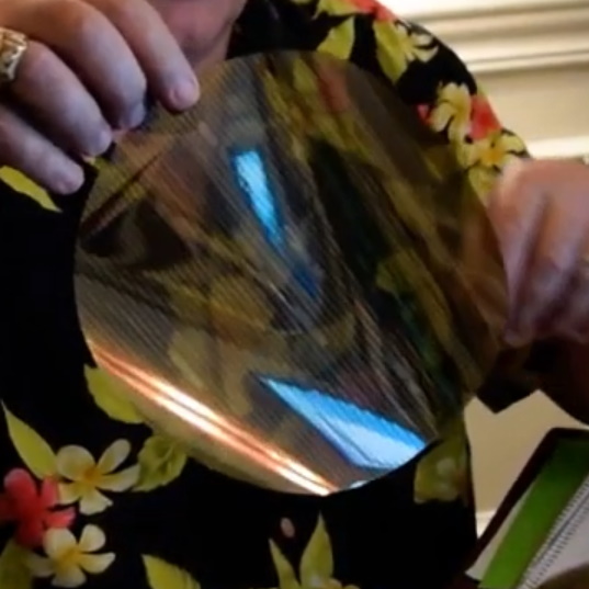
All of which leads us to the guys and gals at PragmatIC Semiconductor. As opposed to a wafer formed from an expensive slice of silicon, they start with an inexpensive glass wafer that’s less than 1 mm thick and 200 mm (approximately 8 inches) in diameter. They then deposit a thin film of polyimide onto the wafer, where polyimide is a polymer of imide monomers belonging to the class of high-performance, heat-resistant plastics.
Next, they build the electronics — transistors, logic gates, multiple layers of metallization — on top of the polyimide using a thin film transistor (TFT) process that has been developed from the ground up to target the unique challenges of flexible integrated circuits. Finally, they peel the flexible polyimide sheet containing thousands of flexible ICs (FlexICs) off the top of the wafer. These FlexICs are thinner than a human hair and can be deployed in things like labels that can be attached to just about anything. Meanwhile, the glass wafer can be used over and over again.
As you can see in this video, the chaps and chapesses at PragmatIC Semiconductor were kind enough to send me one of their wafers so I could experience it up close and personal.
How easy is it to design these FlexICs? Pretty darned easy, let me tell you. First of all, the folks at PragmatIC Semiconductor have their own standard cell library of digital logic gates and functions. They also have their own process design kit (PDK). All of this is compatible with standard industry design tools and flows.
Ken (remember that this is a story about Ken) tells me that the way in which people access FlexIC technology depends on how savvy they are and how many devices they require. The most common option is to use PragmatIC’s own FlexIC Foundry Service. In this case, Ken says, “non-technical users can come to us with a sketch of a circuit on a napkin and we will convert that sketch into their dream.” The next step up is to provide the folks at PragmatIC with a circuit diagram captured using an industry-standard schematic capture package. Alternatively, users can provide an RTL netlist in Verilog that they’ve already simulated and/or prototyped in an FPGA. The little scamps at PragmatIC will even accept a GDSII file, which is the de facto industry standard for data exchange of IC layout artwork.
So, what we are talking about here is the ability to create millions of flexible integrated circuits with an extremely short design cycle, where each FlexIC costs a fraction of a penny. But what about large companies that wish to create billions of such ICs and that want the shortest possible turnaround times with the lowest possible costs? In this case, the little rascals at PragmatIC Semiconductor can set you up with your own FlexLogIC Fab. As we read on the PragmatIC website:
“FlexLogIC is a fully automated FlexIC fabrication line delivering billions of circuits at a fraction of the capital investment and operating cost of a traditional silicon IC fab. FlexLogIC includes all of the required process tools to deposit and pattern multiple high-quality material layers, integrated with a robotic wafer handling system inside a self-contained clean environment. Detailed material recipes, end-to-end process flows, in-line quality monitoring and feedback control loops are implemented within the equipment and automation software, to ensure reliable production without operator intervention.”
I was just watching this video featuring PragmatIC Semiconductor’s CEO, Scott White. As we see, one of PragmatIC’s initial focus areas involves things like near-field communications (NFC) and radio-frequency identification (RFID), which uses electromagnetic fields to automatically identify and track tags attached to objects.
As Scott notes, traditional semiconductor solutions in the form of silicon chips are not well suited to being embedded in thin, flexible form factors. Also, conventional silicon solutions are expensive, which results in their being used only on relatively high-value items or promotional campaigns.
By comparison, the fact that PragmatIC’s FlexICs each cost only a fraction of a cent means that they can be easily embedded into everyday items, enabling the potential for trillions of smart objects. This allows a unique digital identity to be embedded in every object, along with the ability to track that object all the way through the product life cycle, from source manufacturer, through the supply chain, into a retail environment, and on into the consumer’s engagement with the product, all the way through to the product’s end-of-life and recycling.
As Scott notes, this can provide a rich set of data that can be fed into higher level data analytics and artificial intelligence (AI) platforms, which can provide insights into business operations and consumer behavior.
One part of Scott’s presentation that may have caught your attention was where he says that, over time, the folks at PragmatIC are planning on adding sensing and computation capabilities to their offering. All of which brings us back to Ken (remember Ken?) and his mission to track down a 4-bit microcontroller.
I forgot to mention that, in addition to the regular logic gates and register elements in PragmatIC’s standard cell library, they also have SRAM and non-volatile memory (NVM) functions. Based on this, I can easily envisage an RFID-based FlexIC waking up, taking a reading from a temperature sensor, for example, using its microcontroller to perform some simple computations, reporting the results, and then going back to sleep again.
A low-power 4-bit microcontroller would be ideal for this task, but where can you find one that’s fully documented, open source, and royalty-free? Well, this is where Joe Farr and yours truly come in with our 4-bit HRRG microcontroller. In addition to the microcontroller itself, we also have a fully developed assembly language, an assembler, and an associated PC-based simulator.
Of course, nothing has been set in stone and no promises have been made, but — as you can imagine — Joe and I are jolly excited about the possibility of our microcontroller making an appearance in trillions of smart objects. I shall, of course, be reporting further in future columns. In the meantime, as always, I welcome your comments, questions, and suggestions.


Disappointed not to find any link to your “4-bit Heath Robinson Rube Goldberg (HRRG) microcontroller” in this article, or even on this website. And NO, I haven’t heard about it, so keep talking ….
Got here from http://www.ganssle.com/tem/tem413.html The Embedded Muse 413, Jack Ganssle, January 4, 2021.
I’m so sorry — I just now saw this comment — I agree, this may be a good time to bring everyone up to date with the current state of our Heath Robinson Rube Goldberg (HRRG) 4-bit Computer project… watch this space…