

Two and a half decades after deciding that I wanted to live in Silicon Valley, the opportunity to move there finally presented itself. I’d been visiting the area since joining HP in 1975, and Silicon Valley was clearly the epicenter of electronics innovation during the last quarter of the 20th century. When the opportunity came in 1999, my family was living in Boston. We uprooted and moved 3000 miles from the Right Coast to the Left Coast.
Although never my intention, I’ve now worked at several Silicon Valley companies playing in the electronics arena: publishing companies, semiconductor companies, IP companies, EDA companies, and software companies representing a good cross section of employers in the area. I worked in several towns up and down the lower San Francisco peninsula, and my commute was usually about 30 minutes from my home in downtown San Jose, as long as I stayed off the main roads and freeways. That’s very unusual in Silicon Valley.
Here are six vignettes covering my two decades in Silicon Valley. Along the way, I wore many hats, had many jobs, and learned my share of lessons. I kept the six hats and wore them while photographing the corresponding locations where I’ve worked.
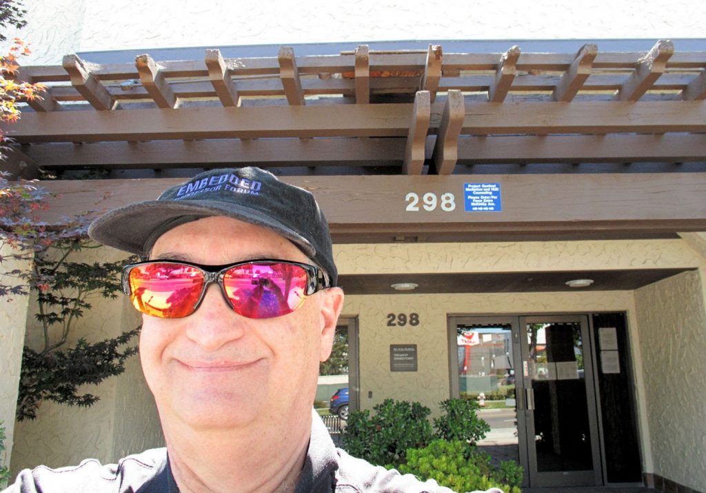
MicroDesign Resources, 298 South Sunnyvale Ave, Sunnyvale, CA
I moved from just outside of Boston to Silicon Valley to start a new publication for MicroDesign Resources (MDR), the publisher of the well-known “Microprocessor Report” newsletter. Founded by Michael Slater in 1987, MDR became a premier source of in-depth microprocessor news and information. Besides publishing “Microprocessor Report,” MDR also staged the annual Microprocessor Forum, a huge event with more than 1000 attendees in peak years. When I joined MDR in 1999, it was operating out of an office that formerly belonged to a Sunnyvale bank. We kept printed back issues of the “Microprocessor Report,” CDs, analyst reports, and swag from the Microprocessor Forums in the bank vault. (It was permanently locked open.)
MDR made its bones on the microprocessor wars. First came the “Intel versus AMD” war, followed by the “RISC versus CISC” and “Arm versus MIPS” (RISC versus RISC) wars. People love to read about conflict; it’s what drives good stories. Vendors announced new, better, and increasingly more exotic microprocessor and DSP architectures every month, and people in the industry wanted to know about them. There were so many new announcements that “Microprocessor Report” couldn’t cover all of them all in each issue, which presented a business opportunity. That’s where I came in. The new MDR publication would cover processors for embedded applications and would be called the “Embedded Processor Report.” Catchy, no?
I’d joined MDR to learn the ropes from Slater, a microprocessor industry legend. Within six months of my joining MDR, Slater, Linley Gwennap, and Keith Diefendorff – the founder, the publisher, and the editor-in-chief – all resigned. Slater quickly got back into startup mode and founded a couple of companies; Gwennap started his own technology analyst firm and purchased MDR in 2010 just prior to it’s being shuttered; Diefendorff went back to working as a microprocessor architect. He’d been an architect on the Motorola Semiconductor 88000 and PowerPC RISC microprocessor projects, and he left MDR to join Apple, which was starting to design its own processors. I was the last manager standing at MDR when these three people left, so I got the publisher and editor-in-chief jobs plus a VP of Content title. The “Embedded Processor Report” idea vanished.
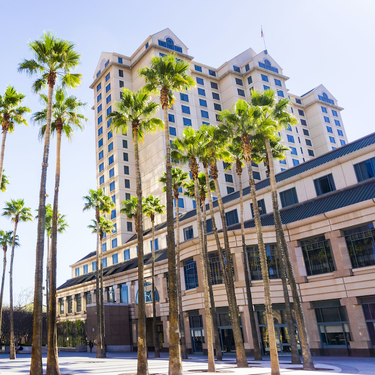
Running the Microprocessor Forum was quite a trip. We filled the entire ballroom at the Fairmont Hotel in downtown San Jose to accommodate the hundreds of attendees who wanted to learn about the latest microprocessors. The Microprocessor Forum had become the premier venue for processor introductions.
Later, the number of attendees shrank, and the Microprocessor Forum no longer filled the Fairmont. Part of the reason for the Microprocessor Forum’s decline was the departure of Intel from the ranks of the event presenters and sponsors. Pat Gelsinger, Intel’s CTO at the time, spearheaded the first Intel Developer Forum (IDF) in 1997, and it became huge, consuming the first few floors of San Francisco’s Moscone Center North – an immense event venue for one company.
With IDF on the rise, Intel soon felt that it no longer needed a 3rd-party event like the Microprocessor Forum for important product launches. Without Intel’s support, attendance at the Microprocessor Forum dwindled. Intel folded the IDF in 2017, but Gelsinger has returned to Intel as CEO and he’s underwriting a similar technology-heavy event, now called Intel Innovation and scheduled for later this year. (More on this below.)
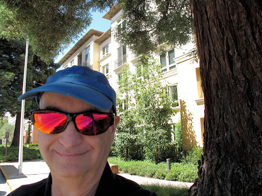
Tensilica, 3255 Scott Blvd, Santa Clara, CA
(Note: The redwood-lined office park that included Tensilica’s one-story building was demolished a few years ago to make room for a new block of condominiums, which were constructed in part from the graveled remains of the older buildings. The new condominiums on the site along with two of the remaining redwood trees appear in the photo.)
Chris Rowen founded Tensilica, a configurable microprocessor IP company, in 1997. He’d been part of the very successful MIPS microprocessor IP startup in the late 1980s that grew out of the RISC processor project at the University of California, Berkeley, led by David Patterson (who coined the term RISC). Silicon Graphics adopted the MIPS architecture for its advanced graphics workstations, and MIPS very effectively competed with the Arm architecture in the RISC wars for many years, until it didn’t.
After MIPS, Rowen founded Tensilica with the idea that every ASIC design team would want to design their own processor with a tailored instruction set if given the right tools, because adding the right special instructions to a microprocessor’s instruction set significantly boosts software execution speed for targeted workstreams. Year by year, Tensilica introduced more capable generations of configurable Xtensa microprocessor IP cores and tools that automatically generated both the microprocessor IP cores and the associated software-development tools from a processor specification written in a proprietary description language called TIE.
Rowen was correct. There were indeed people designing ASICs who wanted to develop their own microprocessors. There just weren’t enough of them. When I joined Tensilica in 2001, the company was supposedly “18 to 24 months” from an IPO. It remained that way for the eight years I worked there.
Tensilica’s management eventually got the message. Most ASIC designers wanted to pick a processor core from a catalog, not design one. That’s the way it worked with Arm processor IP. Tensilica introduced a line of preconfigured “Diamond” processor cores. Some of the Diamond cores like the Xtensa HiFi audio processor sold well.
Tensilica provided rich opportunities for writing about the new configurable microprocessor core concept and for making presentations about the technology around the world. I soon had a collaborator, Grant Martin, who conned persuaded me to write articles and to co-author books with him. I’m forever grateful for Grant’s gentle persuasion. In addition to working with Grant, I helped Tensilica’s CEO Chris Rowen write a book and wrote one of my own: “Designing SOCs with Configured Cores: Unleashing the Tensilica Xtensa and Diamond Cores.” I also started to write blogs for my old magazine, EDN, and I made presentations on Tensilica’s behalf across the United States and in Japan, Korea, the People’s Republic of China, and throughout Europe at various conferences. Working at Tensilica gave me the opportunity to travel the world.
Tensilica exhibited at major events such as the Embedded Systems Conference, the Design Automation Conference (DAC), and Embedded World in Nuremberg. The VP of Marketing, Bernie Rosenthal, always wanted to make a splash at these events, so we developed elaborate booths with scripts to attract audiences. We twice created booths that replicated the bridge of the Starship Enterprise, calling it Starship Tensilica. At another event, we staged flyweight Battlebot duels and surrounded the fighting arena with bleachers. The bleachers were packed for every bout. These skits drew large audiences, and we captured the contact information from every attendee’s badge. When Cadence pulled out of DAC one year, we took their immense exhibit space and turned it into a participatory art studio. Many attendees left the booth smeared with paint.
I learned a lot about the IP business at Tensilica, but all good things come to an end. Tensilica’s inability to reach the financial metrics that would allow an IPO resulted in the replacement of Chris Rowen as CEO. I was laid off shortly after, and the company never had an IPO. Cadence eventually bought Tensilica, as discussed later, and the Xtensa HiFi IP core is still listed in the Cadence IP catalog as Tensilica HiFi DSP cores.
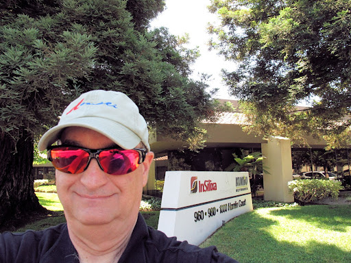
Denali Software, 1000 Hamlin Ct, Sunnyvale, CA
Denali Software became the Switzerland of memory models, used for system simulations. All the memory companies provided their specs to Denali for these models. The company was also famous (or infamous) for the killer parties it threw at DAC. Founders Sanjay Srivastava and Mark Gogolewski had discovered the secret to making their small software company look big. The trick involved copious amounts of alcohol and loud rock music blended together at a cool venue. Everyone likes to have a good time.
After being laid off from Tensilica, I’d started a consulting business for high-tech marketing, and Denali became one of my clients. One of my jobs was writing the “Denali Memory Report,” a definitive newsletter on semiconductor memory. After several months of consulting work, Denali invited me to join full time. On my first day as a full-time employee, I discovered that Cadence Design Systems had purchased Denali during the preceding weekend.
Prior to the purchase, Denali was located in a small, isolated, triangular area in Sunnyvale bordered by the US 101 and CA 237 freeways and Mathilda Ave. There’s only one small entrance to this three-sided plot of land, so I call it Silicon Valley’s Bermuda Triangle. After Cadence acquired Denali, we left the Bermuda Triangle and moved to Cadence’s gleaming white campus in San Jose.
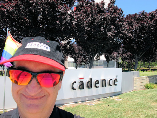
Cadence Design Systems, 2655 Seely Ave, San Jose, CA
Cadence has long been one of the “Big 3” EDA companies focused on IC design. Founded in 1988 through a merger of Solomon Design Associates and ECAD, Cadence was long headed by larger-than-life CEO Joe Costello. Today, Cadence’s CEO is the much less flamboyant Lip Bu Tan, who also serves as the Chairman of the venture capital firm Walden International. Nearly all of the marketing horsepower Cadence needs resides in the two mobile phones that Lip Bu keeps on his belt. He stores the phone numbers of all the CEOs of Cadence’s key customers on those phones.
During my tenure at Cadence, Lip Bu Tan brought in a CMO named John Bruggeman. Although he didn’t know much about EDA, Bruggeman knew a lot about brand marketing. He brewed up a strategic marketing program called EDA360 to put some distance between Cadence and the other two permanent members of the Big 3: Synopsys and Mentor. The EDA360 marketing program worked well because it provided a central rallying point and unifying theme for Cadence’s numerous and disparate EDA product lines, which resulted from the many, many corporate acquisitions Cadence made over the years. Acquisition has been the most typical way that the Big 3 EDA companies have grown.
During the 18 months I spent at Cadence, I expanded my experiments in blogging by writing two concurrent blogs: the EDA360 Insider and the Denali Memory Report. Cadence had decided to retain the Denali name, and the Denali Memory Report had a long history with customers. It fit well into the blog format and maintained Denali’s marketing position as the Switzerland of memory. Meanwhile, the EDA360 Insider blog helped to expand Cadence’s marketing footprint in EDA by making it look as if EDA360 addressed the totality of EDA. Both blogs drew many hundreds and eventually thousands of readers each week.
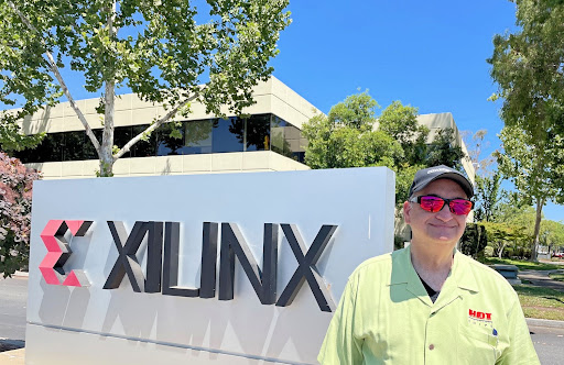
Xilinx, 2100 Logic Drive, San Jose, CA (Photo credit: Shaina Leibson)
I have an old San Jose street map that shows “Corvus Drive” in Xilinx’s current location. In the early 1980s, Corvus Systems bought a small 9-hole golf course in San Jose to build its new headquarters. Back then, Corvus was riding high as a very successful supplier of hard disk systems and Omninet networking hardware for Apple’s early computers. When Ethernet squashed all competing networks, including Omninet, out of existence, Corvus’s business crashed, and the company sold the land and its new building. Xilinx bought it, moved in, built a number of new buildings on the old golf course, and renamed the street. The street sign now reads “Logic Drive.”
Many years later, Steve Glaser, who had become SVP of Corporate Marketing at Xilinx, invited me to join him at Xilinx. He’d met me at Cadence. I agreed to join Xilinx and thus began my deep dive into the FPGA world. I’m originally a systems design engineer, and Xilinx is the first semiconductor company I’ve worked for. However, the FPGA business is its own, very different world.
Effectively, the FPGA business has been a fabless duopoly for many years. Xilinx, founded in 1985, and Altera, founded a year earlier, split the lion’s share of the FPGA market between themselves for decades. Other companies have tried to carve out larger chunks of the FPGA business, but Xilinx and Altera held on tightly.
For many years, new FPGA generations from Xilinx and Altera followed the law of Star Trek movies. Fans of the franchise know that every odd-numbered Star Trek movie (1, 3, 5, 7, 9 …) sucks and the even-numbered movies are the good ones. In the FPGA world, technology leadership seemed to pass back and forth between Altera and Xilinx for each new semiconductor process node.
Xilinx CEO Moshe Gavrielov finally reached the limit of his tolerance for this ping-pong status quo and declared that Xilinx could continue to be the leading FPGA company only by using the world’s leading foundry vendor: TSMC. Prior to this, Xilinx employed a variety of foundries to make its FPGAs. After Gavrielov’s pronouncement, Xilinx used TSMC to manufacture its 28nm Series 7 FPGAs and continues that foundry relationship today.
TSMC was also Altera’s foundry when Gavrielov made his announcement, so Altera decided it needed to pick a foundry vendor that was better than the world’s best. Altera picked Intel, which had superior process technology even compared to TSMC. However, Intel had fine-tuned its process technologies for processors and not for FPGAs. As a result, Altera’s transition to using Intel as a foundry proved somewhat rocky. (Intel subsequently bought Altera in 2015, discussed below.)
Gavrielov placed some big bets, like jumping to TSMC’s somewhat risky 16nm FinFET process technology for the new Xilinx UltraScale+ FPGA architecture, but he hedged the bet by placing the same architecture on TSMC’s 20nm planar process so that Xilinx could introduce the non-plus UltraScale FPGA family a bit sooner, or a lot sooner if the FinFET process proved problematic. Both the original bet and the insurance bet paid off.
Moshe Gavrielov retired at the beginning of 2018, and Steve Glaser left about a month earlier. A week after the new CEO Victor Peng took over, I was laid off.
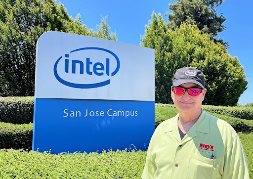
Intel, 101 Innovation Drive, San Jose, CA (Photo credit: Shaina Leibson)
Everyone in the industry knows Intel, whether it’s from the massively effective “Intel Inside” marketing program for PCs, the dancing Bunny Suit television ads, or just the lofty position accorded the semiconductor company that invented both the commercial microprocessor and the commercial DRAM. Intel’s two founders, Robert Noyce and Gordon Moore, are industry giants. The two met in the late 1950s at Shockley Semiconductor Laboratory. They left Shockley and founded Fairchild Semiconductor along with the rest of the Traitorous Eight in 1957, and then the two of them left Fairchild to found Intel in 1968. The semiconductor business literally owes its existence to these two people.
I’d restarted my consulting business after getting laid off at Xilinx and was doing a lot of work for another FPGA vendor, Achronix. Then I got a call from a friend I’d known at Xilinx. She was now at Intel’s Programmable Solutions Group (PSG), the FPGA operation formerly known as Altera, and wondered if I’d like to join her. I said yes. On the day I started at Intel, I discovered that my marketing group would no longer be working for Intel PSG but for Intel’s corporate Sales and Marketing Group (SMG) in the Global Marketing Organization (GMO). (Talk about déjà vu all over again!)
Intel is the largest employer I’ve ever worked for, and its marketing is immensely complex – orders of magnitude more complex than anything I’ve seen in my career previously. Microprocessor launches are planned like large military operations with complex logistics.
With the return of Pat Gelsinger, now Intel’s CEO, the company is restarting IDF, but it’s now called “Intel InnovatiON.” Gelsinger says the purpose of this event is to “bring the geek back to Intel.” Given Gelsinger’s announced plans and public moves, that sounds just about right.
After more than 20 years in Silicon Valley, I’ve retired from Intel. I’m back doing what I love best: writing articles about the most interesting businesses on the planet. See you every week here on EEJournal.com.


