

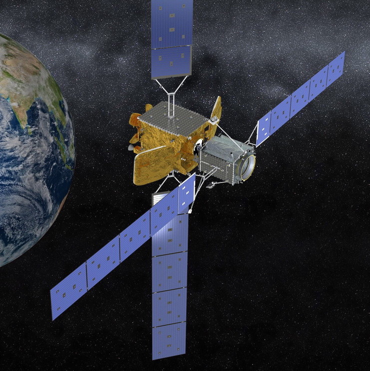
The hot news on the street — if you live on a street where people build satellites and space probes for a hobby — is that those little scamps at Microchip Technology have just announced their new radiation-tolerant (RT) PolarFire FPGA, which they proudly proclaim, “…is optimized to meet the most demanding requirements in spacecraft payload systems’ high-speed data paths with the lowest possible power consumption and heat generation.”
These little rascals (the FPGAs, not the guys and gals at Microchip) boast flash-based FPGA fabric — including memory blocks, DSP blocks, and high-performance SerDes blocks — that is tolerant to radiation-induced configuration upsets in the harshest radiation environments, including space flight (LEO, MEO, GEO, HEO, and deep space), high-altitude aviation, medical electronics, and nuclear power plant control.
Now, you may not immediately think of FPGAs when you hear the Microchip name being bandied around, but — in fact — they now have a respectable FPGA Portfolio, following their acquisitions of Atmel in 2016 and Microsemi in 2018 (remembering that Microsemi had previously acquired Actel in 2010).
We will return to consider these little ragamuffins (again, the FPGAs) in more detail in a moment, but first, let’s briefly remind ourselves as to the different kinds of radiation and radiation-induced effects one might expect to encounter.
Different Types of Radiation
Radiation comes in different forms. One type is electromagnetic radiation (EM radiation or EMR), which spans the gamut from radio waves (low frequency, long wavelength, low energy), through microwaves, infrared, visible light, ultraviolet, and X-rays, to gamma rays (high frequency, short wavelength, high energy).
The force carrier for electromagnetic radiation is a massless particle called a photon. If the photon has a frequency in the ultraviolet or higher, then — when it interacts with an atom or molecule — it can impart enough energy to strip away an electron, thereby leaving a positive ion. Thus, this is referred to as “ionizing radiation.”
Another form of radiation comes in the form of particles: electrons (also known as beta particles, symbol = β), protons, neutrons, and atomic nuclei, where the atomic nuclei can range from helium nuclei (also known as alpha particles, symbol = α) to heavier ions. If a particle is travelling with sufficient speed (which equates to having sufficient energy), then — when it interacts with another atom or molecule — it can act as ionizing radiation and can cause all sorts of undesirable effects.
It’s also common to hear the term “Cosmic Rays”; however, the use of ray in this context is an historical accident, as cosmic rays were initially, and incorrectly, thought to be mostly electromagnetic radiation in the form of X-rays and gamma rays. Cosmic rays are, in fact, very high-energy particles, mainly originating outside the Solar System from cosmic events such as supernova.
Just to provide a sense of scale, as it were, the highest-energy cosmic rays observed thus far have energies comparable to the kinetic energy of a baseball travelling at 90-kilometers-per-hour (56 mph), so you can only imagine what one of these little terrors would do to an integrated circuit (“silicon chip”). When a primary cosmic ray hits the Earth’s atmosphere, it may produce showers of secondary particles that penetrate the atmosphere and sometimes even reach the surface of the planet.
Radiation-Induced Effects
In the case of silicon chip, there are a variety of Single Event Effects (SEEs) that can be triggered by an individual radiation event. One is Single Event Latchup (SEL), in which the radiation event causes a short-circuit between the power and ground rails inside the chip. If an SEL condition occurs, the power has to be cycled (turned off and then on again), but there are techniques that can be built into the chip to mitigate against SELs occurring in the first place.
If a radiation event “flips” a register bit or memory cell (i.e., changes its contents from a 0 to a 1, or vice versa), then this is referred to as an SEU (Single Event Upset). If a radiation event causes a primitive logic gate to generate a pulse on its output, then this is referred to as an SET (Single Event Transient). If the SET is subsequently clocked into the downstream register and/or violates a setup or hold parameter causing that register to enter a metastable condition, then the SET may be converted into an SEU.
Configuration Memory vs. Other Memory Elements
When it comes to FPGAs, there are different memory elements we have to worry about. Let’s start by reminding ourselves that the thing that defines FPGAs is their programmable fabric, which I always think of as “small islands of logic” in a “sea of interconnect.” In fact, someone at one of the larger FPGA vendors once jokingly told me that, “we only charge for the interconnect — we throw the logic gates in for free.”
Each “island of logic” contains a number of elements, including a look-up table (LUT), a multiplexer, and a register element. The operation of each of these elements is defined by a bunch of switches called configuration cells. Similarly, the way in which the “islands of logic” are connected to each other, and to the FPGA’s primary inputs and outputs, is controlled by a humongous number of configuration cells.
As you can imagine, if a radiation event flipped the state of one of your configuration cells, thereby changing the function of your FPGA, the result may not be pretty.
There are three main types of configuration cells: antifuse, flash, and SRAM-based. Antifuse-based configuration cells are totally impervious to radiation, but they are one-time programmable (OTP), which means that, once you’ve programmed your FPGA, there’s no going back, which sort of removes most of the advantages of using an FPGA in the first place.
Flash-based configuration cells are relatively immune to radiation events. In addition to being non-volatile, which means the device is instant-on, Flash-based FPGAs can be reprogrammed as required.
SRAM-based configuration cells have their own advantages and disadvantages. One big disadvantage is that these cells are susceptible to being flipped by radiation events, although there are design strategies that can be employed to mitigate against these effects.
In addition to the configuration cells, the FPGA will also contain blocks of SRAM memory comprised of millions of cells, along with hundreds of thousands of registers. Each of these memory cells and registers is susceptible to radiation-induced SEUs, which must be addressed one way or another (we will return to this point in a moment).
Introducing RT PolarFire FPGAs
In addition to radiation, building systems destined for use in space — like satellites and space probes — involves all sorts of problems, not the least of which is getting rid of any heat they generate. Since the system is operating in vacuum, conduction is not an option, so radiation is the only solution, but you want to keep the radiators as small and lightweight as possible, which means minimizing your power consumption. The folks at Microchip claim that their RT PolarFire FPGAs offer “the lowest possible power consumption and heat generation.”
In the case of imaging applications, satellite operators are demanding more information from their space assets, increased sensor resolution, higher frame rates, and more channels used for multi-spectral imaging. As a result, the raw data is outstripping the available download bandwidth. Rather than simply transmitting humongous amounts of raw data, the solution is to process the images locally (on the satellite) and transmit only useful information.
RT PolarFire FPGAs are ideal for these sorts of space applications. First, they provide significant logic capacity and processing resources in the form of 481k logic blocks, 33 Mbits of SRAM memory, 1,480 DSP blocks, and 24 x 10 Gb/sec SerDes channels.
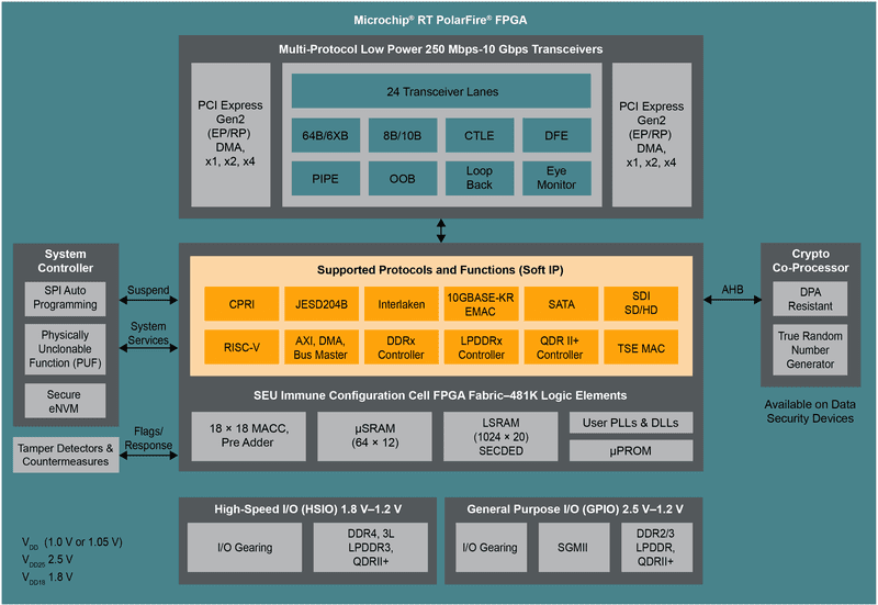
RT PolarFire FPGA block diagram (Image source: Microchip Technology)
RT PolarFire FPGAs use flash-based configuration cells based on SONOS (Silicon-Oxide-Nitride-Oxide-Silicon) technology, which makes them practically immune to radiation events, but what about their SRAM cells and register bits? Well, this is where things get interesting.
The large SRAM blocks (LSRAM) have built-in ECC (error-correcting code), which means they perform error detection and correction (EDAC). This ECC employs single error correct, double error detect (SECDED). In the case of the smaller, micro SRAM blocks (uSRAM), Microchip provides an IP core that implements ECC if this is required. Although it is theoretically possible for a data word to have a multiple-bit radiation-induced error that could defeat the ECC, the probability of this occurring is extremely small.
On top of the ECC, it’s possible to use a small amount of the programmable fabric to implement memory scrubbing, which involves using a background process to read from each memory location, using the ECC to correct any bit errors, and writing the corrected data back to the same location.
One thing the designers have to consider is the relative importance of each potential radiation-induced error. Suppose the satellite is taking high-resolution images at a high frame rate. Now suppose a radiation event flips a single bit in the image memory. In this case, the worst thing that can happen is that the color of a single pixel may be affected, and this will probably “come out in the wash” when passed through the image processing algorithms.
Of course, there are other areas of the design that are mission-critical, such as the navigation parameters and thruster control algorithms. In such cases, these portions of the design can be protected using the synthesis engine to implement triple modular redundancy (TMR).
Having said all this, one of the things that really interests me about these devices is that they are based on Microchip’s commercial 28nm PolarFire die, which means designers can prototype their systems using low-cost commercial parts. The RT dice differ from their commercial counterparts by modifications to their upper metal layers to facilitate integration into their hermetically sealed ceramic packages.
Furthermore, these packages use 1mm pitch column grid array (CGA) technology. Column grid arrays are required because the coefficients of thermal expansion are different between the ceramic package and the circuit board to which it is attached, and systems deployed in space undergo repeated and rapid changes in temperature.
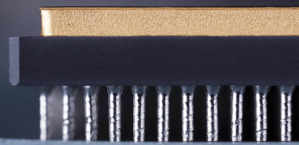
RT PolarFire ceramic packages with CGA technology (Image source: Microchip Technology)
Now, I’ve long been familiar with the concept of CGA technology. However, remembering that we are talking about a 1mm pitch, I was amazed to discover that each column is individually wrapped with a copper spiral, which is itself covered with a layer of eutectic solder (I wouldn’t like to be the man who has to build these columns by hand). I’ve since been informed that this is standard practice for space-bound systems that undergo massive amounts of vibration on their journey into space, followed by the aforementioned thermal cycling. The copper spirals prevent any problems that could be caused by solder columns cracking.
According to the chaps and chappesses at Microchip, their RT PolarFire RTPF500T FPGA will be available and qualified for space-flight deployment in 2021. The great thing is that, as I noted earlier, RT PolarFire FPGAs are based on commercial dice, which means designers can commence prototyping with the commercial PolarFire MPF500T FPGA using Microchip’s Libero software tool suite. These tools include optional triple-mode redundancy (TMR) synthesis support for implementing SEU mitigation where required, such as in control circuits.
Development boards are available with the commercial PolarFire FPGA and will later include the RT PolarFire device in engineering model form. Available radiation data includes TID, SEL, configuration upsets, and upsets in unprotected D-flip flop (DFF) and memory (for more information, feel free to visit the RT PolarFire web site and tell them Max sent you).


