


Microchip now offers a Flash-based microcontroller with an integrated programmable-logic block for less than half a dollar in volume. The nine members of the Microchip PIC16F13145 family (the ‘113, ‘114, ‘115, ‘123, ‘124, ‘125, ‘143, ‘144, and ‘145) sport the same 8-bit RISC microprocessor architecture as other members of the 16F family, but they also incorporate a new programmable-logic block called a Configurable Logic Block (CLB). Devices in the PIC16F13145 microcontroller family are available in 8-, 14, and 20-pin packages with 3.5 to 14 Kbytes of Flash memory and 256 to 1024 bytes of RAM.
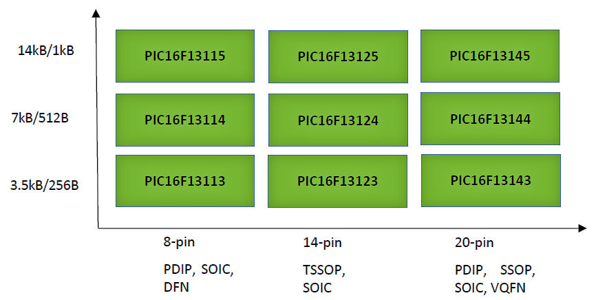
The nine members of the Microchip PIC1613145 microcontroller family have the same internal architecture but feature different amounts of RAM and Flash memory and are offered in different packages, depending on your application’s I/O needs. Image credit: Microchip
The devices in this family have the same types and number of peripherals but differ in the number of external I/O pins, depending on the package. Microchip has incorporated a programmable-logic peripheral called the Configurable Logic Cell (CLC) in its microcontrollers for more than a decade. The CLB in the PIC16F13145 family is a larger and more complex chunk of programmable logic than found in the CLCs incorporated into earlier Microchip PIC and AVR microcontrollers, and I suspect we might see CLBs grow even larger in future PIC16 generations. For backward compatibility, the PIC16F13145 microcontrollers also incorporate four CLCs.
Before delving into the complex innards of the PIC16F13145 devices, I think it’s important to explain how you might use the CLB and to provide some example uses, because it can be somewhat difficult to understand how pairing a low-end microprocessor core chugging along at 8 million instructions/sec with a small, 32-LUT chunk of programmable logic can somehow be far more useful than either component on its own. The CLB comes in handy for implementing a small amount of hardware-level, real-time processing when the PIC16F13145 microcontroller’s CPU proves too slow for the task or when you need some form of simple parallel processing that exceeds the microcontroller’s multitasking abilities.
These sorts of applications are fundamental to why we started using FPGAs in the first place, and Microchip has now transplanted a tiny FPGA – albeit bigger than the older CLCs – into one of its microcontroller subfamilies. You can use the CLB to implement state machines or “high-speed” peripherals such as a software-driven signal multiplexer, counters, a quadrature decoder, a stepper-motor controller, or a high-speed PWM (pulse-width modulator). The CLB can make logical decisions while the CPU is in sleep mode, which can reduce a system’s overall power consumption. The CLB’s outputs can drive external device pins or the inputs of the microcontroller’s other peripheral devices.
The CLB itself looks very much like the programmable logic fabric in an FPGA. The 32 basic logic elements (BLEs) that comprise the CLB closely resemble the logic cells in the first FPGA: the Xilinx XC2064, introduced in 1985. Each BLE consists of a 4-input LUT and a D flip-flop. Wide multiplexers feed sixteen input selection latches that then drive the CLB’s LUT inputs with one of 40 different input signals drawn from external input pins, bits from internal registers, and output pins from internal peripherals. The output of each of the 16 input selection latches feeds into programmable edge detectors. These edge detectors are triggered by positive edges by default but can be programmed to be triggered by negative edges or bypassed completely. Eight more multiplexers route the eight CLB output bits to external pins, to internal registers, or to the inputs of internal peripheral devices. The CLB also incorporates a 3-bit hardware counter, to help build state machines with the CLB, for example.
Microchip’s documentation doesn’t discuss the CLB’s internal wiring, its switch matrix, or its configuration bits. You don’t need to know about them. These details aren’t meant to intrude on the designer’s consciousness. Instead, the MPLAB Code Configurator (MCC), a free software plug-in within the company’s MPLAB X integrated development environment (IDE) software, handles the CLB configuration details based on the designer’s schematic diagram. You create designs for the PIC16F13145’s CLB using a schematic editor integrated into the MPLAB IDE.
All FPGA designs originally employed schematic capture until the FPGAs became too large and complex for schematics. HDL coding in Verilog or VHDL started to eclipse schematic entry in the early 1990s as FPGAs got larger. My good friend Robert Bielby recalls that hierarchical, text-based HDL descriptions had largely displaced schematic entry for FPGA design by the early 2000s, when maximum FPGA capacity was already being measured in thousands of LUTs. (Bielby spent roughly a quarter of a century working in the FPGA business at Altera and Xilinx. Few engineers can remember when designers defined FPGAs with schematics. However, Bielby and I do.)
The largest schematic design Bielby remembers seeing required more than 30 D-sized sheets of paper. That’s awfully big for a schematic. Microchip’s schematic-based approach to CLB design is a throwback to a somewhat distant era in the electronics industry, but it’s still entirely appropriate for an FPGA with 32 LUTs. The PIC16F13145 microcontroller’s 32-LUT CLB is so simple that schematic entry is all that’s required. (Out of curiosity, I’ll ask you: What’s the largest schematic diagram you’ve seen for an FPGA design? Please leave your answer in the comment section.)
Schematic entry for the CLB uses basic symbols such as 2-, 3-, and 4-input logic gates, D or JK flip-flops, 2- or 4-input multiplexers, and simple integer constants. (You might want to pull out your copy of Don Lancaster’s TTL Cookbook for some long-forgotten design recipes.) It’s also possible to work directly with the CLB’s 4-input lookup-tables, which are its fundamental logic elements. Some of the microcontroller’s hardened peripherals can also be included in the design so that the CLB can interact with those on-chip peripheral devices. The CLB can also interact with the microcontroller’s CPU through a register interface, with software-accessible input and output registers appearing as bit-level inputs and outputs on the schematic.
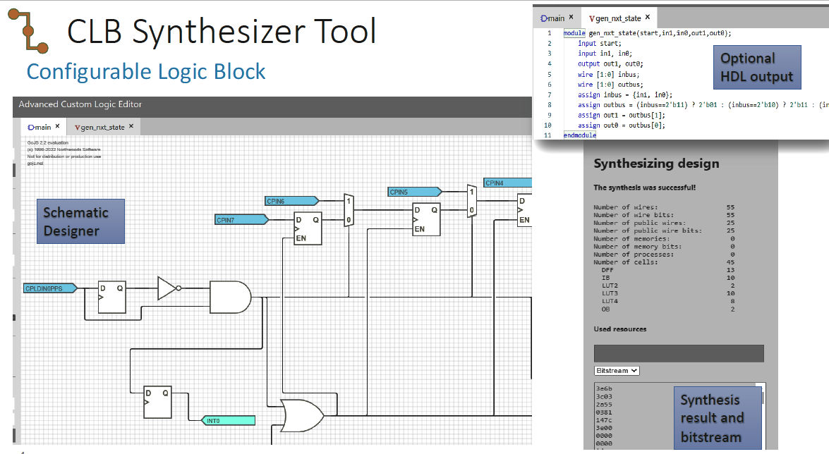
Microchip’s CLB Synthesizer for the PIC16F13145 microcontroller’s programmable logic accepts schematic-level designs (left) and has provision for accepting HDL code as well (upper right). Image credit: Microchip
MPLAB converts the schematic design into a Verilog HDL description prior to synthesizing the design using the MPLAB Code Configurator (MCC). Microchip has made it possible to insert your own Verilog code into a CLB schematic through a block-level container. Once synthesized, MPLAB maps the design onto the CLB, places and routes the design, and generates a configuration bitstream that’s ready to be integrated with the microcontroller’s compiled object code. The CLB configuration is stored as a sequence of constants in the microcontroller’s Flash memory and transferred automatically to the CLB via DMA at boot time. The RAM-based CLB is reconfigurable, so it’s possible to store multiple CLB configurations in the microcontroller’s Flash memory. The microcontroller can reconfigure the CLB under software control. The reconfiguration time is 206 instruction cycles, which is slightly under 26 microseconds at the microcontroller’s maximum 32MHz clock rate.
MCC also provides a GUI-based method for configuring the other peripherals incorporated into the PIC16F13145 microcontroller subfamily. The PIC16F13145 microcontroller incorporates many other peripheral devices in addition to the programmable-logic CLB. All PIC16F13145 microcontrollers include four of the older and simpler programmable-logic CLCs, for backwards compatibility with other Microchip microcontrollers. In addition, the PIC16F13145 microcontroller has a long list of internal peripherals including:
- One 10-bit, 100ksamples/sec ADC with a 22-input analog multiplexer
- One 8-bit DAC
- Two analog comparators
- Two capture/compare/PWM modules with 16-bit resolution for timing and event triggering and 10-bit resolution for PWM
- Two 10-bit PWM modules
- One configurable 8/16-bit timer, one 16-bit timer, and one 8-bit timer
- One UART
- One synchronous serial peripheral with SPI and I2C modes
- One external interrupt pin
- Two selectable voltage references for internal use by the ADCs
Microchip has developed a Curiosity Nano Evaluation Board for the PIC16F13145 microcontroller. It’s about the size of a 40-pin DIP and comes with solderable pin headers. The board connects to a host system via a USB cable and can program the on-board PIC16F13145 microcontroller’s Flash memory by itself. No external programmers are required. Microchip currently sells the Curiosity Nano PIC16F13145 Evaluation Board for the unusual price of $24.02.
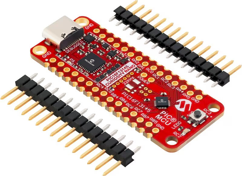
The low-cost Curiosity Nano PIC16F13145 Evaluation Board allows you to explore the microcontroller’s capabilities and can program the Flash memory on the microcontroller through the eval board’s USB port. Image credit: Microchip
The unit price for Microchip’s PIC16F13145 microcontrollers starts at $.47 each in 10,000-unit quantities for the smallest device. The FPGA fabric in the PIC16F13145 microcontroller family is a paltry 32 LUTs, which is roughly half the size of the original Xilinx XC2064 FPGA introduced in 1985. Who knows how many LUTs Microchip might add if the company decided to make a part that sells for $2 in volume.
Although it’s a grossly unfair comparison, you can think of the Microchip PIC16F13145 as a teeny, tiny, twice-removed cousin to the Arm-based processor and FPGA combo SoCs sold by AMD and Intel. Those chips incorporate multiple 32- or 64-bit Arm processors and thousands of FPGA LUTs. However, many embedded designs don’t need nearly that amount of processing power, but they often do need more performance than is available from a software-driven, 8-bit microcontroller. That’s where the low-cost Microchip PIC16F13145 with its small integrated FPGA might provide just the capabilities you need.
Related articles in EEJournal
A History of Early Microcontrollers, Part 9: The General Instruments PIC1650
Don Lancaster: The Electronics Industry Lost Another Pioneer Last Year


My actual project for Xilinx (xc6slx25, package ftg256, speed -2) contains:
Slice Registers: 7,089
Slice LUTs: 8,457, used as Memory (RAM, ROM and shift register): 1,333
DSP48A1s: 17
IOBs: 153
Max frequency: 160 MHz
I never print the schematics!
Janos, your project is about 500 times bigger than the FPGA in PIC16F13145. Of course you don’t print the schematics.
The capability of being able to load multiple bitstreams into the microcontroller flash and re-program the CLB on-the-fly is very interesting indeed.
Depending on the application, you could almost use that to extend the capability of the CLB by programmatically switching out the configuration, based on conditions sensed by the microcontroller – almost like having multiple 32 LUT FPGAs, albeit without the capacity to act concurrently.
The ability to reconfigure the PIC16F13145’s small FPGA on the fly is indeed an interesting feature of this device, tanon. I must admit that I can’t think of much more to do with this feature than a signal mux, but Adam Taylor seems enamored of the device and I am certain he’ll come up with some interesting applications for it.
Meh. Had rhey been serious about it, they’d bolted it on AVR, not PIC16 core.
PiC16 is a crime against humanity and PIC18 is not much better.
This is just a niche product for some customer that they thought they might try selling to others.