


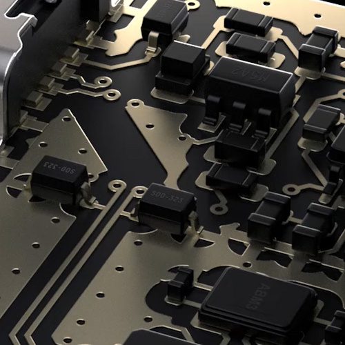
I want you to close your eyes and imagine something. I’ll tell you when you can open them again. Hmmm, that won’t work, will it? OK, let’s try something different. Imagine you’ve closed your eyes and you are visualizing a printed circuit board (PCB) from the future, except the ‘P’ is a misnomer because this board is not “printed” per se.
Let’s come at this from a different direction. Do you remember the 1991 movie, Terminator 2: Judgment Day? One of its stars is an advanced, shape-shifting Terminator—a model T-1000, no less—that’s made of virtually indestructible liquid metal. I’m thinking about the scene where the T-1000 simply oozes through the steel bars blocking a corridor in the prison where Sarah Connor is being held. I still have goosebumps.
Well, keeping the T-1000 in mind, imagine a circuit board whose liquid-metal tracks and vias can be reconfigured on demand. “This is all very Buck Rogers in the 25th Century,” I hear you say, “but what does it have to do with the here and now?” I’m so glad you asked, or else I would have been obliged to think of some cunning way to bring what I’m about to tell you into the conversation.
In a crunchy nutshell, a company called Itera has just emerged from deep stealth mode to announce a new circuit board technology whose liquid-metal tracks and vias can be… you’ve guessed it… reconfigured on the fly before your very eyes.
In case you were wondering, Itera takes its name from Iterate, which is particularly pertinent because we tend to do a lot of that during the prototyping phase of a new project.
Speaking of prototyping, I’ve certainly served my time. Considering only professional activities, I started in the early 1980s with hand-soldering wires onto rudimentary prototype boards carrying naught but plated-through holes and pads. Later, the company I worked for adopted a technique called “wire wrap,” which was originally invented to wire telephone crossbar switches and later adapted for constructing electronic circuit boards. Robert Jenkins has a great video of this on his technology channel.
Later still, we acquired (or rented, I’m not sure which) a monstrous Multiwire machine. In this case, the board’s surface was covered with a layer of adhesive wiring film. A special computer-controlled wiring machine was used to ultrasonically bond extremely fine wires into the wiring film. These wires had an insulating polyimide coating and could be wired orthogonally (north-south, east-west), diagonally, or in combination. Since the wires were insulated, they could cross without forming unwanted connections.
I remember a crowd of us setting this machine running in the evening before heading home. When we reconvened in the morning, our new Multiwire prototype board was ready for us to populate with components to find out what we’d done wrong on our design. Although this may sound like a lot of effort, it was better than waiting two or three weeks for a prototype PCB to arrive from the local board house.
One more thing before we proceed: the folks who create circuit boards enthusiastically mix and match units as though it were a competitive sport. For example, it’s common to specify track widths and spacings in units of “mils,” where one mil equals 1/1000th of an inch. The term derives from the Latin mille, meaning “thousand,” which explains why generations of engineers and machinists have colloquially referred to it as a “thou.”
Because modern electronic components (excluding legacy through-hole devices) have mostly transitioned to metric pin spacing, it is extremely useful to know standard conversions, such as 1 mil = 0.001 inches and 1 mm = approximately 39.37 mils. Just for giggles and grins, some people talk in microns (millionths of an inch). For the purposes of this column, it’s worth knowing that 100 microns is approximately 4 mils.
Last but not least, standard low-cost PCBs typically have 6-mil line-and-space (trace width and spacing) rules; mid-range boards are usually in the 4–5-mil range; and advanced boards push down into the 2–3-mil realm.
I just had a very interesting, if not mind-boggling, chat with AJ Cooper, who is CEO and Co-founder of Itera. At first glance, Itera’s technology looks like something that escaped from a science-fiction movie. The company’s prototype board isn’t built from FR4 fiberglass and copper traces. Instead, it’s formed from multiple layers of ultra-thin glass containing microscopic channels through which liquid metal can be directed to create traces and vias on demand. The entire structure is sealed, so the liquid metal is never exposed to the outside world. Take a look at this visualization of Itera’s fluid circuit board technology in action.
One way to visualize this is to imagine a circuit board as a two-dimensional array of pixels. In a conventional display, each pixel can be turned on or off. In Itera’s board, each pixel can either contain liquid metal or remain empty. When neighboring pixels are filled, the metal joins together to form a conductive trace. Every pixel can also act as a vertical interconnect, allowing metal to flow between layers and create a via whenever required.
The really clever part is that all of this movement is controlled by thin-film transistors distributed throughout the glass substrate. The result is a circuit board whose routing can be compiled, erased, and recompiled in seconds rather than being permanently etched into copper. This visualization gives a better feel for how the tracks and vias are formed.
If you’re wondering what prevents the liquid metal from simply sloshing back into a puddle the moment power is removed, think of the electronic ink used in a Kindle e-reader. Once its pixels have been set to black or white, they remain that way without requiring continuous power. Itera’s liquid metal behaves in much the same way. Once traces and vias have been formed, they remain in place even after the control electronics are turned off. The board effectively “remembers” its routing configuration until instructed to change it.
If all of this sounds vaguely familiar, perhaps it’s because we’ve seen something similar before. Field-programmable gate arrays (FPGAs) allow engineers to configure logic in the field. Itera’s technology allows engineers to configure the physical interconnect itself. As AJ put it during our conversation, “It’s essentially a field-programmable metal array (FPMA) in three dimensions.” That’s not merely a catchy phrase. It’s a reasonably accurate description of what’s going on inside the board.
Although the board may be exotic, assembling electronics onto it is surprisingly familiar. The liquid metal never comes into direct contact with components. Instead, permanent conductive structures connect internal routing pixels to pads on the surface of the outermost glass layers. Conductive adhesive or conductive paste is deposited onto selected pads, and standard pick-and-place equipment positions conventional surface-mount components exactly as it would on a traditional PCB. From the component’s perspective, it has been mounted on an ordinary circuit board. The magic happens underneath.
An unexpected side effect (well, I certainly wasn’t expecting it) of embedding switching electronics throughout the substrate is that the board can also act as its own measurement instrument. Traditional PCBs allow engineers to probe only locations they had the foresight to expose as test points. Internal traces are often inaccessible. By comparison, Itera’s architecture allows engineers to observe electrical activity throughout the board, including locations that would normally be buried inside inner layers. The company says engineers can effectively probe any region of the design and even create temporary measurement paths as needed. For anyone who has ever spent days hunting an elusive signal-integrity problem hidden deep inside a multilayer board, this is a very intriguing proposition indeed.
Before anyone starts imagining full-sized server motherboards built from shape-shifting liquid metal, it’s worth noting that Itera is still at the beginning of its journey. The current proof-of-concept device is a single-layer board roughly 70 mm square with a routing pitch of 200 microns (about 8 mils). The next milestone is to implement a two-layer version with 100-micron (4-mil) pitch. Once two layers are working reliably, additional layers can be stacked using the same architecture, eventually reaching layer counts commonly found in modern commercial designs. The company ultimately sees panel sizes growing toward roughly 350mm × 350mm.
One surprising aspect of Itera’s announcement is that the company’s initial product isn’t a board you buy. Instead, the founders describe it as “AWS for electronics.” Engineers submit their design files and bill of materials. Itera assembles the specified components onto one of its reconfigurable substrates, compiles the routing to match the design, and then provides secure remote access to the hardware. Engineers can interact with the system through interfaces such as USB, UART, Ethernet, cameras, test instrumentation, and internal measurement capabilities as though the hardware were sitting on the bench in front of them. When a change is required, the design is simply recompiled instead of waiting weeks for a new PCB spin.
In the longer term, it’s easy to imagine a future in which a compact version of this technology sits on every engineer’s workbench, allowing hardware developers to iterate on physical designs almost as quickly as software developers iterate on code. The founders certainly believe that’s where this technology could eventually lead.
I bet you’re skeptical. We’ve all seen supposedly revolutionary ideas come and go without sticking to the wall, as it were. What makes Itera particularly interesting is that it appears to have moved well beyond the “wouldn’t it be cool if…” stage. The company has already demonstrated working hardware and raised a $12 million seed round. More importantly, its initial production capacity has already been reserved by major players in the automotive, defense, hyperscale computing, and semiconductor sectors.
AJ says these organizations are reluctant to identify themselves publicly because they view faster hardware iteration as a genuine competitive advantage. As far as I’m concerned, that’s perhaps the strongest endorsement of all. When potential customers start treating your existence like a state secret, you may be onto something.