


Bill Hugle and Frances Sarnat married in 1947 after each had earned an undergraduate degree in chemistry at the University of Chicago. The two started a business making artificial gemstones in 1948, but the venture went bust by 1951 because of a patent infringement lawsuit brought against Bill Hugle by Linde Air Products, which had hired him as a plant chemist in 1947, just before he started his side business with his wife. The Hugles wanted to continue working together and, after receiving many rejections to employment inquiries, were able to secure employment with the DH Baldwin Piano Company of Cincinnati, Ohio.
Baldwin introduced its first electronic organ in 1946. This organ was based on Winston Kock’s design from the 1930s, which used a bank of oscillators constructed from neon gas-discharge tubes, capacitors, resistors, and inductors. (See “Winston Kock: Right Place, Right Time, Right Idea.”) Baldwin’s chief competitor in the electronic organ market was Hammond, which used electromechanical tone wheels and inductive pickups to generate multiple tones. In the 1940s, Baldwin started to experiment with tone wheels using optical disks instead of the metal ones that Hammond used. These disks transcribed tones into photolithographically etched patterns on the glass disks. When the disks spun, the etched patterns translated into electrical waveforms using optical sensors that read the patterns from the disks.
It’s not clear that Baldwin ever introduced an organ that used these optical tone wheels, but the US Army Signal Corps recognized that the technology could be used for a completely different purpose – optical shaft encoders – which would be very handy for pointing radio and radar antennas. The US Army Signal Corps issued a contract to Baldwin for the development of optical encoders in 1951. By 1953, Baldwin had produced a 16-bit optical device under this contract. That was the same year that Baldwin hired Bill and Frances Hugle and moved them to Cincinnati.
Of course, this coincidence alone does not prove that the Hugles worked on the optical encoder development project, but consider the patents issued to Frances and Bill Hugle and assigned to Baldwin during their employment at that company:
Semi-conductive films and methods of producing them, Patent Number US2994621A, filed March 29, 1956
“As is well known, various metals and semi-metals including cadmium, tellurium, lead, zinc, germanium, indium, antimony, selenium, mercury, silicon, and sulfur, are capable of forming in various combinations photoelectric or semi-conductive films, which have utility in electrical apparatus. The present invention applies to all of these. However, great difficulty has been encountered in the past in forming films of combinations of metals or semi-metals. For example, if a cadmium selenide film is desired, it has been usual to produce the cadmium selenide first in the form of crystals and then vaporize the crystals to form the films. Such a method is in general elaborate, time-consuming, costly, and in some instances involves serious operational hazards.
“It is an object of the invention to provide a method for the direct production of semi-conductive films of metals or semi-metals which will be cheaper and more convenient than methods hitherto current in the art.”
Methods of etching metals in the platinum group and producing printed circuits therefrom, Patent Number US3013956A, filed April 5, 1957
“Recently, printed circuit techniques have been applied to the fabrication of photocells. ln accordance with these techniques, an electrically conducting coating is disposed upon an electrically insulating substrate or base, and a resist is disposed upon the coating of electrically conducting material in the desired pattern to form two confronting spaced electrodes. The entire assembly is then immersed in a bath of solvent which removes the portion of the electrically conducting coating which is not protected by the resist. The resist is then removed, leaving two confronting spaced electrically conducting electrodes on an electrically insulating base. A mass of photoconductor material, generally of the semiconductor class, is then disposed on the base between the electrodes and in Contact with the electrodes, this step generally requiring the application of heat. The patent application of the present inventors entitled Semi-Conductive Films and Methods of Producing Them, Serial No. 574,804, filed March 29, 1956, illustrates photocells constructed in this manner.
“lt is often desirable that the confronting electrodes of a photocell constructed in this manner be spaced by a small distance. As a result, the mass of photoconductor material extending between the electrodes is also small.
“lt is one of the objects of the present invention to provide a method of dissolving metals in the platinum group with a solvent which will not substantially attack conventional resist materials. lt is a further object of the present invention to provide a method for etching such metals. provide an etching process for fabricating printed circuits with platinum group conductors.”
Method of producing a photocell assembly, Patent Number US3187414A, file February 5, 1959
“The present invention relates to photocells and methods of manufacturing photocells. This application is a continuation-impart of application Serial No. 574,804, entitled Semi-Conductive Films and Methods of Producing Them, filed March 29, 1956, now Patent No. 299,4621.
“In recent years, optical encoders have been developed which employ an assembly of photocells in combination with a light source and a code disc disposed between the light source and photocell assembly to produce a binary output representing the angle of the code disc. Application Serial No. 631,818 of William Pong entitled Encoder, filed December 31, 1956, now Patent No. 3,076,959, is an example of such an encoder. As pointed out in the Pong application, the sensitive areas of each of the photocells are desirably extremely small in order to avoid the use of a readout slit between the code disc and the photocell assembly.
“Although the present invention will be illustrated as applied to an optical encoder, it is to be understood that photocell assemblies have many utilities in addition to optical encoders, such as devices for reading out information on punched cards.”
These three patents leave little to the imagination. It’s very clear that the Hugles were deeply involved in the development of optical encoders at the DH Baldwin Piano Company, and specifically in the development of thin-film photocells and photocell arrays for those encoders. This image from the Hugle family archives provides additional evidence:
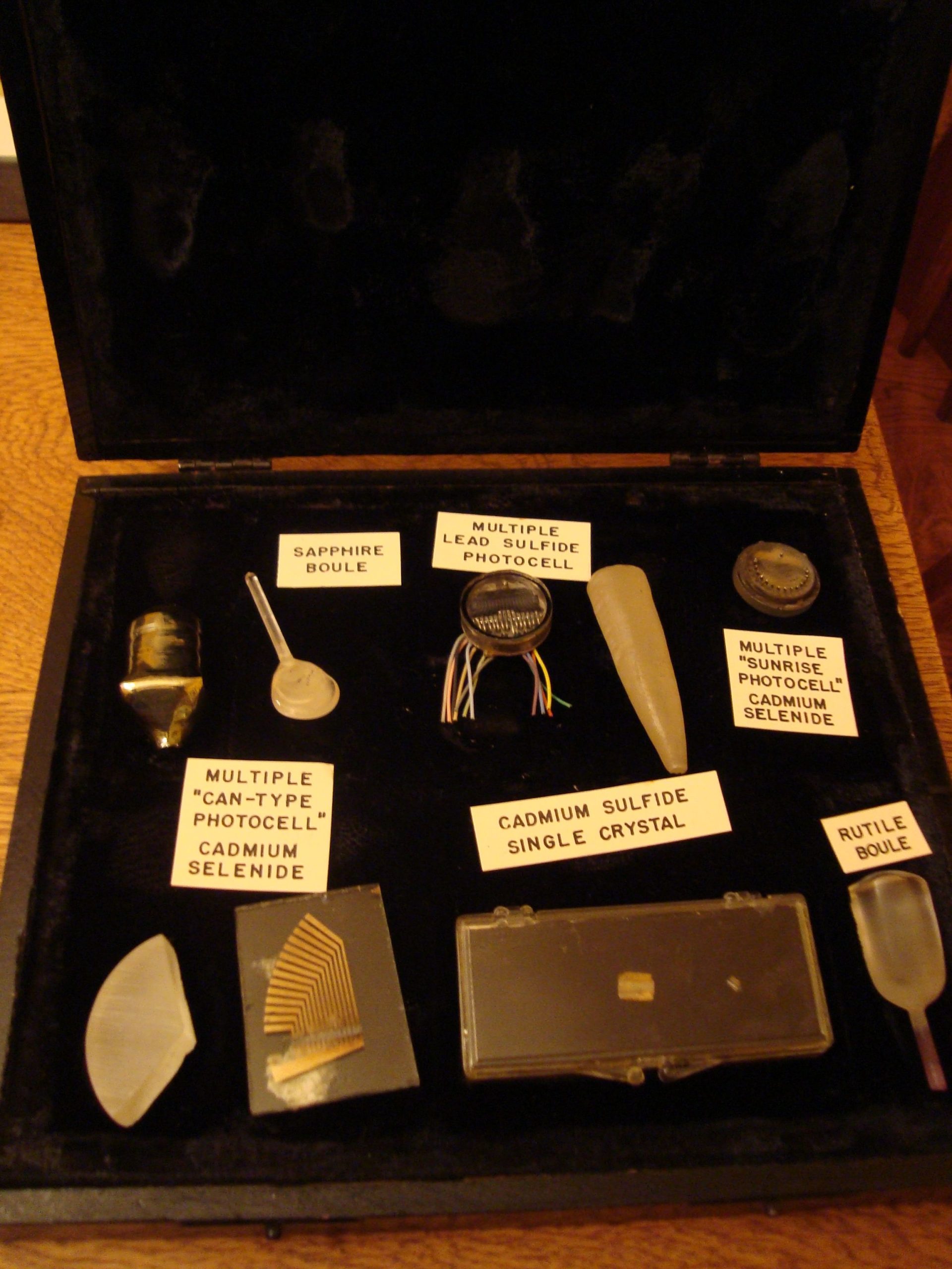
Photocells and crystal boules produced by Bill and Frances Hugle while working for the DH Baldwin Piano Company. Image credit: Jacob Loomis
The above image clearly shows a connection between the sapphire (aluminum oxide) and rutile (titanium dioxide) gemstone boules produced by the Hugles during their previous venture and the cadmium sulfide crystal and the lead sulfide and cadmium sulfide thin-film photocells and photocell arrays they developed for Baldwin.
Baldwin produced the first experimental optical encoders for the US Army Signal Corps in 1955. The company subsequently acquired American Radio and Television, a company located in Little Rock, Arkansas, to serve as Baldwin’s electronics manufacturing center. By 1960, all of Baldwin’s encoder manufacturing was being done in Little Rock. In 1962, Baldwin developed an 18-bit optical encoder that was used in American spacecraft. A year later, the company produced the first optical encoder with an LED light source, specifically for space applications. That same year, Baldwin incorporated its electronics division as Baldwin Electronics, Inc, which is often referred to by its initials, BEI. In 1974, Baldwin Electronics became an independent company through a sale to 33 of its employees, backed by San Francisco venture capitalist Charles Crocker. The new company’s name became BEI Electronics Inc.
The Hugles left Baldwin on good terms long before BEI became an independent company. During their work with Baldwin, the Hugles added to their knowledge about and experience with semiconductor thin films, photolithography, and chemical etching, at least as it applied to circuit boards. Bill left Baldwin in 1958 and went to Youngwood, Pennsylvania, just outside of Pittsburgh, to help Westinghouse build a semiconductor cleanroom, possibly to be used at least partially by Westinghouse’s new Solid State Advanced Development Laboratory, which was working under a new Molecular Electronics development contract with the US Air Force. Frances joined Bill in Pennsylvania some months later with their children. This move marks the Hugles’ first full step into the semiconductor business, which is the subject for Part 3 of this article series.
Note: This history of Frances and Bill Hugle is sparsely documented on the Internet,and this series of articles would not have been possible without the aid and assistance of the Hugles’ grandson, Jake Loomis, and the founder of TechSearch, Jan Vardaman, who was instrumental in creating an IEEE Scholarship program in the name of Frances Hugle, which was funded in part by Jake Loomis’s mother and Frances Hugle’s daughter, Linda Hugle.


Indeed, Baldwin Piano and Organ did produce and sold organs based on optical tone wheels. These were called their Multi-Waveform Organs. I believe one of these organs was built into Cincinnati’s Music Hall as I recall a fellow Baldwin Piano and Organ Company employee pointing out the two panels far above the stage that were slightly recessed to allow the organ’s speakers to have a clearer means to make their sound.
rrestel, thanks for the comment. The documentation I have seen said the Multi-Waveform organ did not go into production. Is there any documentation that you know of showing it became a production product. The presence in Cincinnati’s Music Hall (same town as Baldwin) suggests, but doesn’t prove, that it was a production product.
rrestel, thanks for the comment. The documentation I have seen said the Multi-Waveform organ did not go into production. Is there any documentation that you know of showing it became a production product. The presence in Cincinnati’s Music Hall (same town as Baldwin) suggests, but doesn’t prove, that it was a production product. It looks like some foundation contributed that organ to the Music Hall. In addition, I’ve seen some blog traffic suggesting that the Multi-Waveform organ did not use optical technology. Those are the reasons I wrote what I did.
…looking into what I can find. -RR